Silicon-based multi-layer cavity filter

A cavity filter and silicon-based technology, applied in waveguide devices, electrical components, circuits, etc., can solve the problems of inability to meet the miniaturization requirements of the system, the processing accuracy cannot be satisfied, and the difficulty of system integration to achieve small radiation loss , Improve device performance, easy to realize the effect of complex structure

Active Publication Date: 2012-02-22
THE 13TH RES INST OF CHINA ELECTRONICS TECH GRP CORP
View PDF5 Cites 57 Cited by
  • Summary
  • Abstract
  • Description
  • Claims
  • Application Information

AI Technical Summary

Problems solved by technology

Although the performance of the traditional cavity filter is good, the volume is too large to meet the miniaturization requirements of the system
In order to realize the miniaturization of the system, a cavity structure filter based on a dielectric substrate and a low temperature co-f

Method used


Image

  • Silicon-based multi-layer cavity filter
  • Silicon-based multi-layer cavity filter
  • Silicon-based multi-layer cavity filter

Examples


Embodiment 1

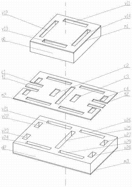
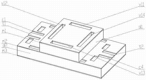
[0022] Depend on figure 2 with image 3 It can be known from the shown embodiment 1: a silicon-based multilayer cavity filter, the filter is composed of an upper dielectric layer d1 and a lower dielectric layer d2 made of high-resistance silicon, and the upper dielectric layer d1 is provided with a filter that satisfies the resonance condition The first to fourth through holes v11, v12, v13, and v14 formed by silicon micromachining technology, and the fifth to thirteenth through holes formed by silicon micromachining technology that meet the resonance conditions are arranged on the lower dielectric layer d2. Holes v21, v22, v23, ..., v29, the shape of the through hole is rectangular (or square, circular, long); on the inner wall of the through hole, there is an inner wall formed by silicon micromachining technology. Metal layer; an intermediate metal layer m2 is provided between the upper dielectric layer d1 and the lower dielectric layer d2, and the intermediate metal layer...

Embodiment 2

[0025] Depend on Figure 4 with Figure 5 The shown embodiment 2 shows: a silicon-based multilayer cavity filter, the filter is composed of a top dielectric layer D1, a second dielectric layer D2 and a bottom dielectric layer D3 using high-resistance silicon, and the first dielectric layer D1 The first to ninth through holes V11, V12, ..., V19 are provided on the top, the tenth to sixteenth through holes V21, V22, ..., V27 are provided on the second dielectric layer D2, and the third dielectric layer D3 is provided with seventeenth to twenty-third through holes V31, V32, ..., V37, the shape of the through holes is rectangular (or square, circular, long strip), the inner wall of the through hole The inner wall metal layer is provided by silicon micromachining technology, and the first intermediate metal layer M2 is provided between the top dielectric layer D1 and the second dielectric layer D2. The first intermediate metal layer M2 is provided on the silicon micromachining tec...

Embodiment 3

[0029] The difference from Example 2 is that the first intermediate metal layer is composed of an upper part and a lower part, and the upper part is provided on the lower surface of the upper dielectric layer adjacent to the first intermediate metal layer through silicon micromachining technology On the top, the lower part is provided on the upper surface of the lower dielectric layer adjacent to the first intermediate metal layer through silicon micromachining technology; the upper part and the lower part are provided with the same shape (or different shape) at the same position ) interstage coupling window. The upper part and the lower part of the first intermediate metal layer are respectively connected to form the first intermediate metal layer through a bonding process in silicon micromachining technology.

[0030] In the present invention, the shape of the through hole on the dielectric layer can be rectangular, square, circular or long; the metal layer in contact with t...


PUM


Abstract

The invention discloses a silicon-based multi-layer cavity filter, which is formed by superposing more than two medium layers up and down, wherein a through hole is formed in each medium layer; an internal wall metal layer which is formed by using a silicon micro-machining technology is arranged on an internal wall of the through hole; an intermediate metal layer which is formed by using the silicon micro-machining technology is arranged between the two adjacent medium layers; an inter-stage coupling window is arranged on the intermediate metal layer; an upper surface of a top medium layer and a lower surface of a bottom medium layer are respectively provided with a surface metal layer which is formed by using the silicon micro-machining technology; a metal layer which is contacted with the upper and lower surfaces of each medium layer and an internal wall metal layer form a resonant cavity; and an input tap lead is arranged on one resonant cavity, and an output tap lead is arranged on another resonant cavity. The silicon-based multi-layer cavity filter is small in size, has a shielding function, can meet the accuracy requirement of microwave/millimeter wave frequency band, and is free from encapsulation, good in device consistency, compatible with an integrated circuit process, easy to implement system integration and convenient to assemble and debug.

Description

technical field [0001] The invention relates to a microwave filter applied in the field of wireless communication, in particular to a silicon-based multilayer cavity filter with a through-hole structure based on silicon micromachining technology. Background technique [0002] Filters are widely used in electronic systems such as satellites, communications, aviation, and aerospace. As an important component of electronic systems, their miniaturization is the biggest bottleneck in realizing the miniaturization of electronic systems. Although the traditional cavity filter has good performance, it is too bulky to meet the miniaturization requirements of the system. In order to realize the miniaturization of the system, a cavity structure filter based on a dielectric substrate and a low temperature co-fired ceramic (LTCC) has appeared, but its processing accuracy cannot meet the accuracy requirements of the device in the microwave / millimeter wave frequency band, and it is difficu...

Claims


Application Information

Patent Timeline
IPC IPC(8): H01P1/207H01P1/208
Inventor 杨志杨拥军胡小东李倩
Owner THE 13TH RES INST OF CHINA ELECTRONICS TECH GRP CORP
Why Eureka
Try Eureka