


Quick Research
Generate reliable direction feasibility study reports for your R&D in just a few steps.

Technical Q&A
Discover and master advanced knowledge NOW. Basics, ideas, possibilities, all at once.

Find Solutions
As an expert in R&D theories, this can generate solutions to your technical problems instantly.

Evaluate Feasibility
Analyze your overall solution with one click, know your potential R&D risks in advance.

Monitor Landscape
Get weekly tech updates, stay abreast of the latest tech innovations and key insights.
Suspension photoresist planarization technology for MEMS structure
A planarization process and photoresist technology, which is applied in the field of planarization technology and photolithography, can solve problems such as few researches, and achieve the effects of simplified process flow, material saving and simple method
- Summary
- Abstract
- Description
- Claims
- Application Information
AI Technical Summary
Problems solved by technology
Method used
Image

Examples
Embodiment 1
[0020] This embodiment is a method for fabricating an Al micro-beam structure by using a suspension photoresist planarization process.
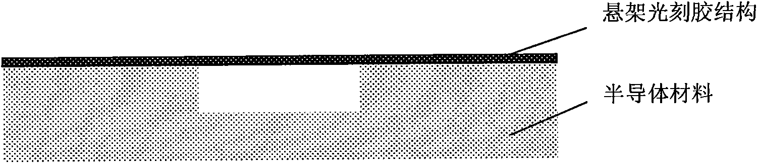
[0021] Cantilever beams and double-end fixed beam structures are often required to be fabricated in MEMS devices. The traditional manufacturing method is usually to make the shape of the microbeam on the flat lower surface first, then etch the release groove on the lower material around the edge of the microbeam, and finally use the isotropic etching method to corrode and hollow out the lower material to release the microbeam structure. This manufacturing process limits the sequence of micro-beams first and then release, and a series of complex and expensive processes such as surface planarization are required to fabricate micro-beam structures in the case of pre-existing grooves. The application of the suspension photoresist realizes the process steps of the groove first and then the microbeam structure, which makes the manufacturing proces...
Embodiment 2
[0029] This embodiment is a method for manufacturing the suspended electrode at the end of the cantilever beam by using the suspension photoresist planarization process.
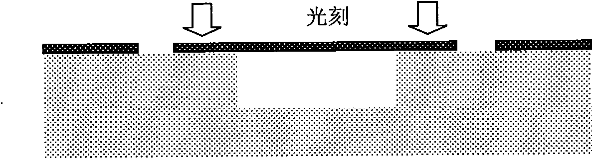
[0030] In the MEMS structure, it is often necessary to make a new suspended structure on the suspended structure, such as the current detection structure of the metal layer at the end of the cantilever beam. The floating electrodes must be fabricated after etching the cantilever beam to release the groove, and due to the existence of the groove steps at the end of the cantilever beam, the fabrication of the metal floating electrodes must use a planarization process. see Figures 4a-4f , its specific process steps are as follows:
[0031] (1) Cantilever beams are etched on silicon wafers and passed through XeF 2 Processes such as release make it a suspended structure, and other components can be made according to requirements.
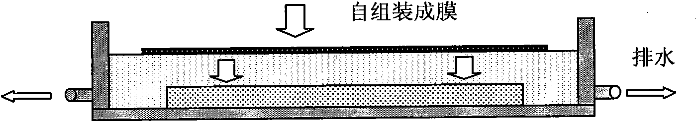
[0032] (2) Self-assemble AZ5214 photoresist on the surface of deionized water ...
Embodiment 3
[0037] This embodiment is a method for manufacturing fixed-point connection electrodes across trenches by using the suspension photoresist planarization process.
[0038] see Figures 5a-5d , in the MEMS process, it is sometimes necessary to connect metal electrodes across the intermediate structure and across the trench between two separated structures. The suspension photoresist planarization process of this method provides convenience for the fabrication of this structure. Its specific implementation steps are as follows:
[0039] (1) Make the AZ5214 photoresist self-assemble on the surface of deionized water to form a photoresist film with a thickness of about 500nm, and then transfer it to the pre-fabricated Figure 5a On the top layer silicon-silicon oxide-silicon substrate triple layer structure (SOI substrate) of the shown structure, so that it forms a suspension photoresist structure spanning the gap structure in the top layer silicon.
[0040] (2) Exposing and deve...
PUM
 Abstract
Description
Claims
Application Information
 - R&D Engineer
- R&D Manager
- IP Professional
- Industry Leading Data Capabilities
- Powerful AI technology
- Patent DNA Extraction
Browse by: Latest US Patents, China's latest patents, Technical Efficacy Thesaurus, Application Domain, Technology Topic, Popular Technical Reports.
© 2024 PatSnap. All rights reserved.Legal|Privacy policy|Modern Slavery Act Transparency Statement|Sitemap|About US| Contact US: help@patsnap.com