

Enhanced high electron mobility transistor and manufacturing method thereof
A manufacturing method and transistor technology, applied in semiconductor/solid-state device manufacturing, circuits, electrical components, etc., can solve problems such as poor performance of enhanced gallium nitride transistors, and achieve the effect of improving poor performance and increasing threshold voltage
- Summary
- Abstract
- Description
- Claims
- Application Information
AI Technical Summary
Problems solved by technology
Method used
Image

Examples
Embodiment Construction
[0044] In order to enable your review committee to have a further understanding and understanding of the characteristics, purpose and functions of the present invention, the detailed description is as follows in conjunction with the drawings:
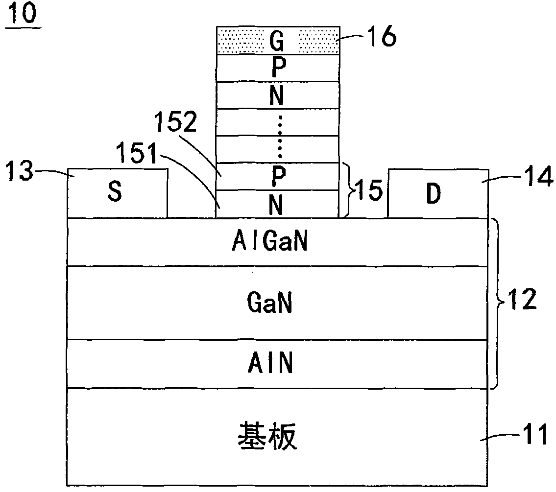
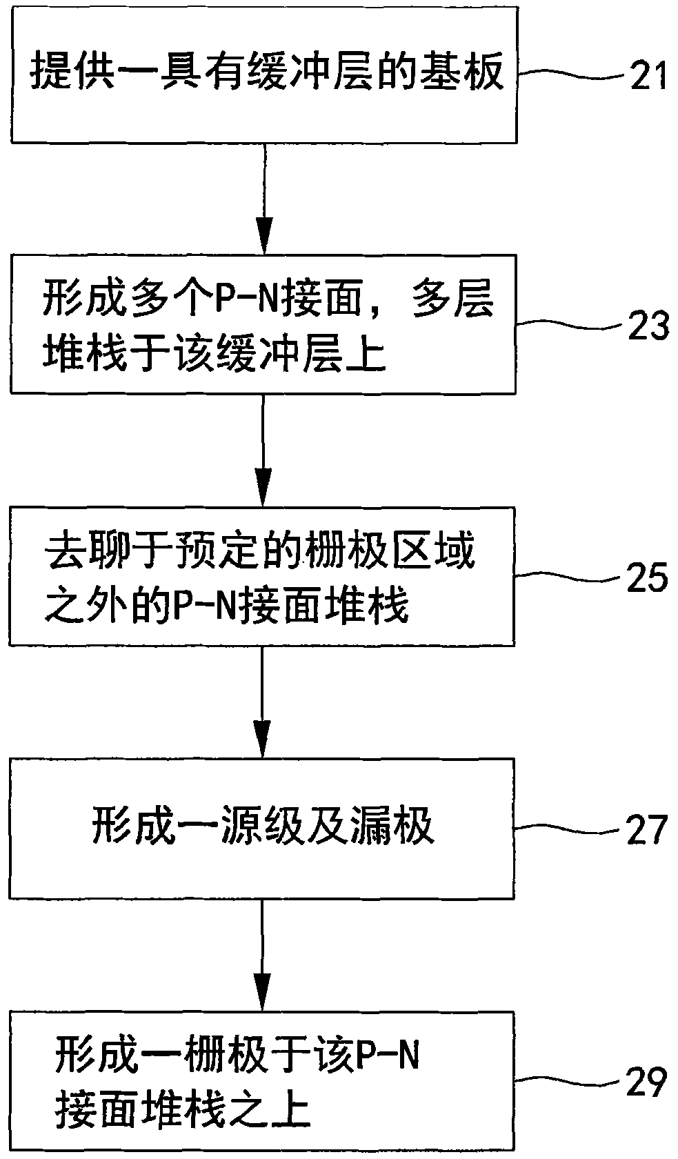
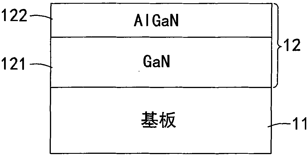
[0045] Please refer to figure 1 , is a cross-sectional schematic view of an embodiment of an enhanced high electron mobility transistor with multiple PN junctions according to the present invention. As shown in the figure, the enhanced high electron mobility transistor 10 of this embodiment structurally includes: a multilayer stack of a substrate 11, a buffer layer 12, a source 13 and a drain 14, and a plurality of P-N junctions 15 , and a grid 16 . The substrate 11 is used to support the semiconductor elements constructed thereon, and its material is not particularly limited, and may be gallium arsenide (GaAs), gallium nitride (GaN), silicon (Si), silicon carbide (SiC), sapphire (Sapphire), or other semiconductor materials. A buffer...
PUM
 Abstract
Description
Claims
Application Information