Method for preparing graphene nanoribbon on insulating substrate

A technology of graphene nanobelts and insulating substrates, applied in the field of preparing graphene nanobelts and growing graphene nanobelts, can solve the problems that graphene nanobelts cannot be directly prepared, and achieve the effect of avoiding transfer

Active Publication Date: 2012-03-28
SHANGHAI INST OF MICROSYSTEM & INFORMATION TECH CHINESE ACAD OF SCI
View PDF7 Cites 28 Cited by
  • Summary
  • Abstract
  • Description
  • Claims
  • Application Information

AI Technical Summary

Problems solved by technology

[0008] The present invention aims at the shortcomings of directly growing graphene on hBN substrates and other substrates with atomic-level flatness cleavage planes and the inability to directly prepare graphene nanoribbons in the prior art, and proposes an insulating substrate with atomic layer steps. A method for the controllable preparation of high-quality graphene nanoribbons in a step-flow manner on the substrate to meet the needs of preparing transistors and other graphene optoelectronic devices on microelectronics

Method used


Image

  • Method for preparing graphene nanoribbon on insulating substrate
  • Method for preparing graphene nanoribbon on insulating substrate
  • Method for preparing graphene nanoribbon on insulating substrate

Examples


Embodiment 1

[0043] Example 1: Preparation of hexagonal boron nitride substrate with monoatomic layer steps

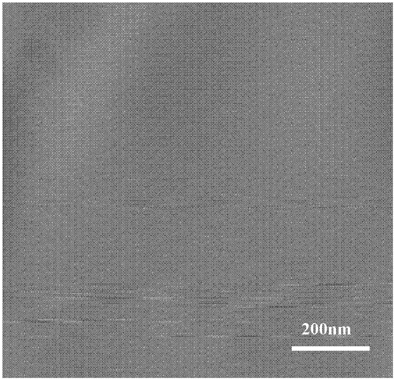
[0044] The first step: using single crystal hBN flakes as raw materials, on SiO 2 / Si substrates were mechanically exfoliated to obtain hBN sheets with fresh cleavage planes, such as figure 1 As shown, its surface is very flat without any steps.

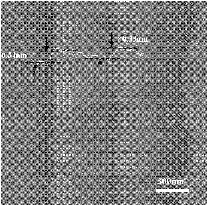
[0045] The second step: the hBN / SiO obtained in the first step 2 The substrate is put into a tube furnace, and the hydrogen-argon gas mixture (H 2 : Ar=1:3, volume ratio), be warming up to 1200 ℃ with the heating rate of 20 ℃ / min, constant temperature 10min, then cool with furnace, obtain like this figure 2 The height of the steps shown in the single atomic layer height analysis shows that the height difference of the steps is 0.34nm and 0.33nm, which is a single BN atomic layer step, and the distance between the steps is about 500nm.

Embodiment 2

[0046] Example 2: Preparation of hexagonal boron nitride substrate with monoatomic layer steps

[0047] The first step: take the single crystal hBN block as the substrate, and remove the surface layer of hBN by mechanical stripping.

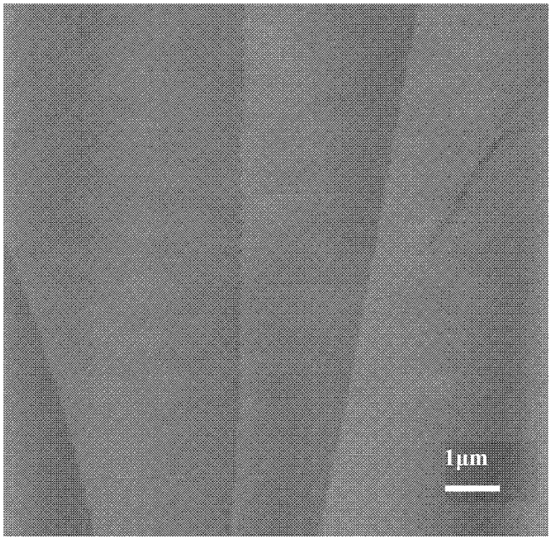
[0048] The second step: the substrate is put into the tube furnace, and the mixed gas of hydrogen and argon (H 2 : Ar=1:6, volume ratio), with a heating rate of 20°C / min, it is heated up to 1100°C, kept at a constant temperature for 50min, and then cooled with the furnace, so that the steps of the monoatomic layer height are obtained, such as image 3 shown. The spacing between the steps is 1-5 microns.

Embodiment 3

[0049] Example 3: Preparation of hexagonal boron nitride substrate with monoatomic layer steps

[0050] The first step: the hBN grown by CVD method is used as the substrate, and the hBN surface layer is removed by mechanical stripping. The process of preparing hBN by CVD method is as follows: use borazine as the BN source, argon as the carrier gas, and grow the hBN film at 1000 ° C on the metal Ni as the substrate under the pressure of 5 Pa for half an hour, and transfer the hBN film to SiO 2 / Si substrate.

[0051] The second step: the substrate is put into the tube furnace, and the mixed gas of hydrogen and argon (H 2 : Ar=1:9, volume ratio), with a heating rate of 20°C / min, it is heated up to 1000°C, kept at a constant temperature for 300min, and finally cooled with the furnace, so that the steps of the monoatomic layer height are obtained, such as Figure 4 shown. The analysis result of the step height is 0.35nm, which is a single BN atomic step, and the interval betwee...


PUM

PropertyMeasurementUnit
widthaaaaaaaaaa
widthaaaaaaaaaa
widthaaaaaaaaaa

Abstract

The invention provides a method for growing a graphene nanoribbon on an insulating substrate of a cleavage surface with atomic scale smoothness, belonging to the field of low-dimensional materials and novel materials. The method comprises the following steps of: firstly, splitting the insulating substrate to obtain a cleavage surface with atomic scale smoothness, and preparing a monoatomic layer step; and secondly, directly growing the graphene nanoribbon by using the insulating substrate with the regular monoatomic layer step. With the adoption of the characteristics of different nucleation powers of the graphene on the atomic step and the smooth cleavage surface, the graphene is ensured to grow into the graphene nanoribbon with adjustable size only along step edges through regulating conditions, such as temperature, pressure intensity, active carbon atom supersaturation degree and the like. The method for preparing the graphene nanoribbon on the insulating substrate is mainly applied to the field of novel graphene photoelectric devices.

Description

technical field [0001] The invention relates to a method for preparing graphene nanobelts on an insulating substrate, in particular to a method for growing graphene nanobelts by using an insulating substrate with a single atomic layer thickness step as a template. It belongs to the field of low-dimensional materials and new materials. Background technique [0002] Restricted by physical principles, the processing limit of silicon materials is generally considered to be a line width of 10 nanometers. If it is less than 10 nanometers, it is unlikely to produce products with stable performance and higher integration. Finding alternative materials for silicon as the channel layer of next-generation optoelectronic devices has become an urgent task to continue Moore's Law and obtain higher-performance chips. Since graphene was discovered in 2004, due to its unique properties, including the thinnest, strongest, high thermal conductivity, high hardness, high electron mobility, zero...

Claims


Application Information

Patent Timeline
Patent Type & Authority Applications(China)
IPC IPC(8): C23C16/26C23C16/02B82Y40/00B82Y30/00
CPCC01B31/0453C01B2204/065B82Y40/00B82Y30/00C01B32/186
Inventor 唐述杰丁古巧谢晓明陈吉王陈江绵恒
Owner SHANGHAI INST OF MICROSYSTEM & INFORMATION TECH CHINESE ACAD OF SCI
Why Eureka
Try Eureka