Solar cell and method of producing same

A solar cell and back electrode technology, applied in the direction of electrical components, final product manufacturing, sustainable manufacturing/processing, etc., can solve the problems of insufficient conversion efficiency, achieve strong and excellent conversion efficiency, prevent electrode peeling, and conduct electricity excellent effect

Inactive Publication Date: 2012-04-11
MITSUBISHI ELECTRIC CORP
View PDF8 Cites 3 Cited by
  • Summary
  • Abstract
  • Description
  • Claims
  • Application Information

AI Technical Summary

Problems solved by technology

[0004] In addition, if the BSF layer is formed by printing and firing the Al paste material on the entire surface of a thin and large-area substrate, in order to prevent warping and cracking of the substrate, the Al paste material may be printed and fired in dots. method, or the method of using BBr3 to form the entire surface by the thermal diffusion method, etc., but if such a method is used, sufficient conversion efficiency cannot be obtained, so as a solution, a planar rear surface is formed on the entire rear surface of the substrate Electric field layer, and a dot-shaped back electric field layer deeper than the planar back electrode is provided at a predetermined position on the back surface of the substrate (for example, refer to Patent Document 2)

Method used


Image

  • Solar cell and method of producing same
  • Solar cell and method of producing same
  • Solar cell and method of producing same

Examples


Embodiment approach 1

[0031] Next, embodiments of the present invention will be described using the drawings. In the following description of the drawings, the same or similar symbols are attached to the same or similar parts. However, it should be noted that the drawings are only schematic diagrams, and ratios of dimensions and the like are different from actual ones. Therefore, specific dimensions and the like should be judged in consideration of the following description. In addition, it is needless to say that the relationship and ratio of mutual dimensions are different between drawings.

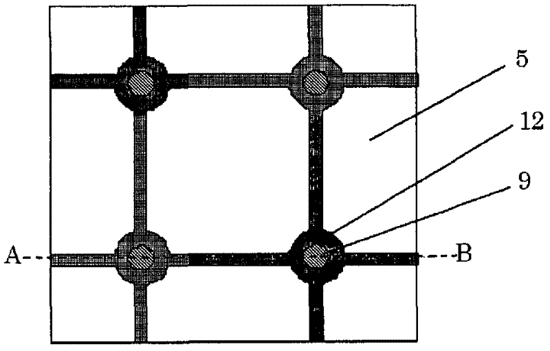
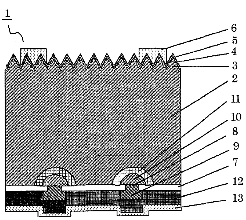
[0032] figure 1 It is a perspective view of a part of the solar battery cell in Embodiment 1 of the present invention seen from the back side (the back side lower layer electrode is shown). in addition, figure 2 is along figure 1 It is a cross-sectional view when A-B shown is cut.

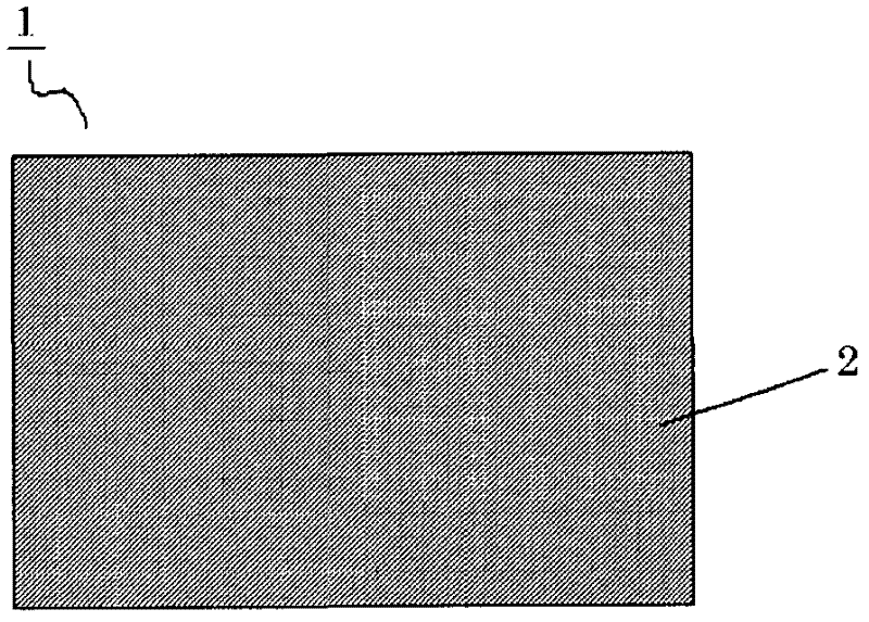
[0033] In the figure, a solar battery unit 1 includes a silicon substrate 2 composed of p-type single crystal or polycry...

Embodiment approach 2

[0051] Figure 14 It is a perspective view of a part of the solar battery cell in Embodiment 2 of the present invention seen from the back side (showing the back side lower layer electrode). In Embodiment 1 above, the case where the aluminum electrode 9 is in the form of dots has been described, but in the solar battery cell with the rear passivation structure of the present invention, if the opening area is reduced in polysilicon, the silicon will be dissipated due to the grain boundary. The response changes and the contact state is unstable, so there is a possibility that sufficient characteristics cannot be obtained.

[0052] Therefore, in the solar battery cell 1 according to Embodiment 2 of the present invention, the shape of the opening to the passivation film 7 and the electrode shape of the aluminum electrode 9 as the first back electrode make it possible to pass through the polycrystalline crystal grain boundaries. The strip-shaped electrodes 14 are configured in a s...

Embodiment approach 3

[0062] In Embodiment 1 described above, the Al-Si paste containing aluminum particles and silicon particles was printed superimposedly on the basis of forming the aluminum electrode to form the Al-Si electrode as the second back electrode, but it is also possible to use aluminum and For the Al—Si alloy obtained by melting silicon, a paste made of powder obtained by making the alloy into particles or a paste containing the powder is used.

[0063]The composition ratio of aluminum and silicon in this Al—Si alloy is the same as the mixing ratio in the case of using aluminum particles and silicon particles, and silicon is 5 to 20 parts by weight relative to 100 parts by weight of aluminum.

[0064] In the case of using a powder made of Al-Si alloy, the reactivity to the silicon substrate is slightly lower than the case of using a paste made of a mixed powder of aluminum particles and silicon particles, so the substrate can be Warpage is suppressed to be small.


PUM

PropertyMeasurementUnit
Surface resistanceaaaaaaaaaa
Thicknessaaaaaaaaaa
Thicknessaaaaaaaaaa

Abstract

Disclosed is a solar cell with high photoelectric conversion efficiency, comprising a semiconductor substrate, a front surface textured section formed on the main surface of the light-receiving surface side of the semiconductor substrate, a semiconductor layer having a conductivity type and formed along the front surface textured section, and an anti reflection film formed on the light-receiving surface side of the semiconductor layer, wherein a passivation film is formed on the main surface of the back surface side of the semiconductor substrate, at least one opening section is provided in the passivation film, and a first back surface electrode, which overlaps all portions on the passivation film in the range occupied by the opening section and covers the opening section, and a second back surface electrode, which overlaps all portions on the passivation film in the range occupied by the first back surface electrode and covers the first back surface electrode, are formed, whereby a partial back surface electrode, which does not suffer from electrode peeling or high resistance of an electrode conductor, is provided on the passivation film. Also disclosed is a method of producing the same.

Description

technical field [0001] The present invention relates to a solar cell unit and a method of manufacturing the same. Background technique [0002] In most conventional crystalline silicon solar cells having a PN junction, an n-type diffusion layer is formed entirely on the main surface (hereinafter referred to as the surface) that is the main surface on the light-receiving surface side of the p-type polycrystalline silicon substrate. , On the light-receiving side of the surface, tiny bumps and surface electrodes are set. BSF (Back Surface Field, hereinafter referred to as BSF) and BSR (Back Surface Reflection) are implemented on the back main surface (hereinafter referred to as the back surface) which is the main surface opposite to the light-receiving surface side of the solar cell unit. , Backside reflection, hereinafter referred to as BSR), by using the reflection of light-generated carriers of BSF and the reflection of incident light by using BSR, the exchange efficiency o...

Claims


Application Information

Patent Timeline
IPC IPC(8): H01L31/04
CPCH01L31/1804H01L31/0236H01L31/068H01L31/03682H01L31/022425H01L31/1868H01L31/028Y02E10/50Y02E10/547H01L31/02363Y02P70/50
Inventor 藤川正洋松野繁
Owner MITSUBISHI ELECTRIC CORP
Why Eureka
Try Eureka