Bonding wire for semiconductor

A bonding wire and semiconductor technology, applied in semiconductor devices, semiconductor/solid-state device manufacturing, electric solid-state devices, etc., can solve the problems of higher specific heat than gold, inability to form spherical parts, and high melting point of palladium, etc., to achieve good Excellent wedging property and oxidation resistance

Active Publication Date: 2012-04-18
NIPPON STEEL CHEMICALL &MATERIAL CO LTD +1
View PDF15 Cites 43 Cited by
  • Summary
  • Abstract
  • Description
  • Claims
  • Application Information

AI Technical Summary

Problems solved by technology

Although the above-mentioned documents do not show the superiority of palladium, since the melting point of palladium is higher than that of silver (melting point 1554°C), and the specific heat of palladium is higher than that of gold (244J / kg·K), it is considered that if palladium is coated, the following problems can be solved. Problem: Like the above-mentioned silver and gold, the coating layer is melted before the copper wire is melted to form the spherical portion, and the spherical spherical portion cannot be formed.

Method used


Image

  • Bonding wire for semiconductor
  • Bonding wire for semiconductor
  • Bonding wire for semiconductor

Examples


Embodiment

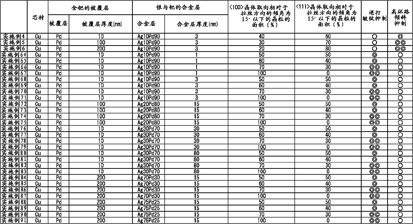
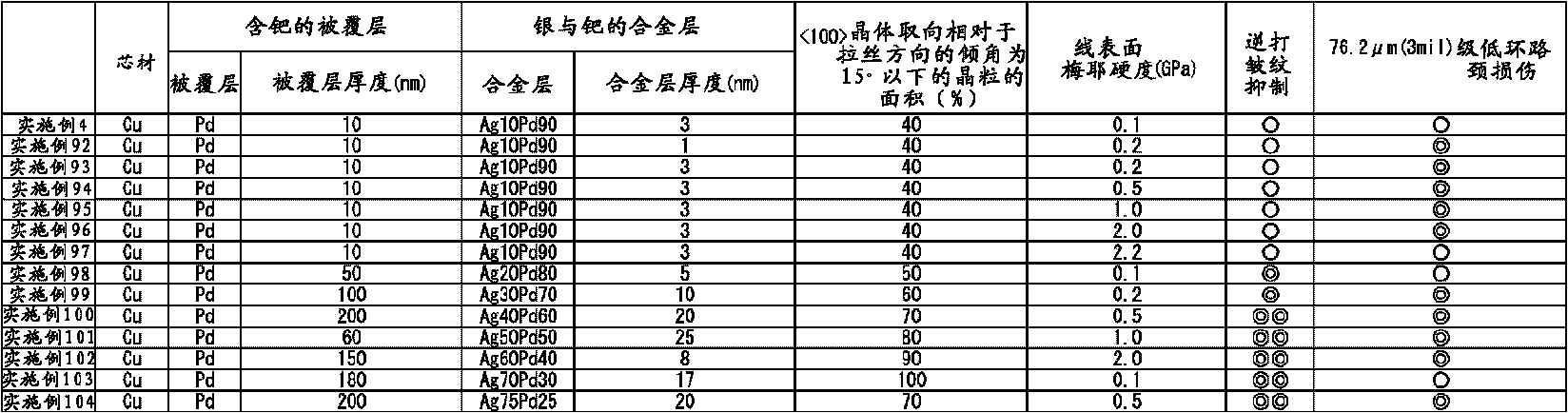
[0094] Hereinafter, Examples will be described.

[0095] First, a production example and evaluation of a bonding wire having an alloy layer containing silver and palladium on the surface of the coating layer will be described.

[0096] As the raw materials of the bonding wire, copper used for the core wire, B, P, Se, Ca, and Al as additive elements in the core wire, palladium used for the coating layer, and silver used for the skin layer, each with a purity of 99.99 was prepared. mass % or more of the billet. After weighing the above-mentioned copper or copper and additive element raw materials as starting materials, they are heated and melted under high vacuum to obtain copper or copper alloy ingots having a diameter of about 10 mm. Then, forging, rolling, and wire drawing were performed to produce a wire having a predetermined diameter. Then, a coating layer containing palladium is formed on the surface of each wire by electroplating. Here, the thickness of the above-ment...


PUM


Abstract

Disclosed is a bonding wire for semiconductor, which ensures good wedge bonding even of palladium-plated lead frames and has excellent oxidation resistance, and in which copper or a copper alloy is used as a core wire. The bonding wire is characterized by comprising a core wire that comprises copper or a copper alloy, a coating layer that is arranged on the surface of the core wire, has a thickness of 10 to 200 nm and contains palladium, and an alloy layer that is arranged on the surface of the coating layer, has a thickness of 1 to 80 nm and contains a noble metal and palladium, wherein the noble metal is silver or gold, and the noble metal is contained in the alloy layer at a concentration of 10 to 75 vol% inclusive.

Description

technical field [0001] The present invention relates to a bonding wire for a semiconductor used for bonding an electrode on a semiconductor element and an external connection terminal. Background technique [0002] At present, as a semiconductor bonding wire (hereinafter referred to as a bonding wire) for connecting an electrode on a semiconductor element and an external terminal, a wire diameter of about 20 to 50 μm and a material of high-purity 4N (4-Nine, with a purity of 20 to 50 μm) are mainly used 99.99 mass % or more) gold (Au) bonding wire (gold bonding wire). In order to bond a gold bonding wire to an electrode on a silicon chip as a semiconductor element, ball bonding by ultrasonic and thermocompression bonding is generally performed. That is, the method is as follows: using a general-purpose bonding device, the above-mentioned gold bonding wire is passed to the inside of a jig called a capillary, the tip of the wire is heated and melted by arc heat input, and a s...

Claims


Application Information

Patent Timeline
IPC IPC(8): H01L21/60C22C5/02C22C5/04C22C5/06
CPCH01L2224/45124H01L2924/0105H01L2224/05624H01L2224/48724H01L2924/01025H01L2224/4851H01L2224/48699C22C5/02H01L2924/15311H01L2224/85045H01L2924/01028H01L2924/01013H01L2224/45015H01L2924/20751H01L2224/85065H01L2924/20753C22C5/04H01L2224/85207H01L2224/48247H01L2924/01033C22C9/00H01L2924/00015H01L2224/85464H01L2924/20755H01L2924/01074H01L2924/01078H01L2224/85444H01L2924/01016H01L2224/4516H01L2924/01015H01L2224/48624H01L2924/01046H01L2924/01082H01L2224/43848H01L2224/85075H01L2924/01004H01L2924/01018H01L2224/45572H01L2924/20752H01L2924/01019H01L2924/01029H01L2224/4312H01L2224/85439H01L2224/45639H01L2924/014H01L2924/01024H01L2224/45147H01L2224/48599H01L2224/78301H01L24/43H01L2924/01047H01L2224/45644H01L2924/01079H01L2224/45565H01L24/45H01L2224/48011H01L2924/01005H01L2924/20754H01L2924/01006H01L2924/0102H01L2224/45664H01L2924/10253H01L2224/85564H01L2924/01014H01L2224/45144H01L2924/01075C22C5/06H01L2224/48799H01L2224/85181H01L2224/48839H01L2224/48844H01L2224/48864H01L2224/48739H01L2224/48744H01L2224/48764H01L2224/48824H01L2224/4321H01L2224/48471H01L2224/85186H01L2924/00011H01L2924/01034H01L2924/00014H01L2924/01204H01L2924/20105H01L2924/20106H01L2924/20107H01L2924/20108H01L2924/01001H01L2924/20756H01L2924/20757H01L2924/20758H01L2924/01007H01L2224/45669H01L2924/2076H01L2224/48465H01L2924/20654H01L2924/20652H01L2924/20655H01L2924/00H01L2924/013H01L2924/20109H01L2924/2011H01L2924/20111H01L21/48H01L21/4864H01L21/4885H01L21/4889
Inventor 寺岛晋一宇野智裕山田隆小田大造
Owner NIPPON STEEL CHEMICALL &MATERIAL CO LTD
Why Eureka
Try Eureka