
Pb-free solder for high-temperature electronic packaging and preparation method thereof

A technology for electronic packaging and lead-free solder, applied in manufacturing tools, welding equipment, metal processing equipment, etc., can solve the problems of poor brazing performance, high tensile strength, difficult processing, etc. good performance

Active Publication Date: 2012-05-02
ZHEJIANG ASIA GENERAL SOLDERING & BRAZING MATERIAL
View PDF7 Cites 6 Cited by
  • Summary
  • Abstract
  • Description
  • Claims
  • Application Information

AI Technical Summary

Problems solved by technology

[0003] At present, there are not many research reports on lead-free high-lead solder. Potential alternative alloys include Au-based, Bi-based, Zn-Al-based, Sn-Sb-based alloys, etc., but these alloys have their own defects.
[0004] Au-based solder is mainly used in optoelectronic packaging, airtight packaging of high-reliability and high-power electronic devices, and chip packaging. Commonly used Au-based alloys include Au-Sn, Au-Si, Au-Ge, etc., but gold-based alloys Hard, high tensile strength, low elongation, difficult to process into wire or strip, and the cost is too high, which limits its application
[0005] Chinese patent application CN155896A proposes to replace high-lead solder with Ag containing BiAg alloy (solidus temperature greater than 262.5°C) of 2-18wt.%. This alloy has large brittleness, poor processability, and brazing performance with Cu and Ni substrates poor
However, when the Sb content is less than 10%, the melting point is low, and the alloy has the problem of rapid corrosion of Cu or Ni substrate pads, and the alloy has poor oxidation resistance, and a large amount of tin slag will be produced in the welding process

Method used


Image

  • Pb-free solder for high-temperature electronic packaging and preparation method thereof

Examples


Embodiment 1

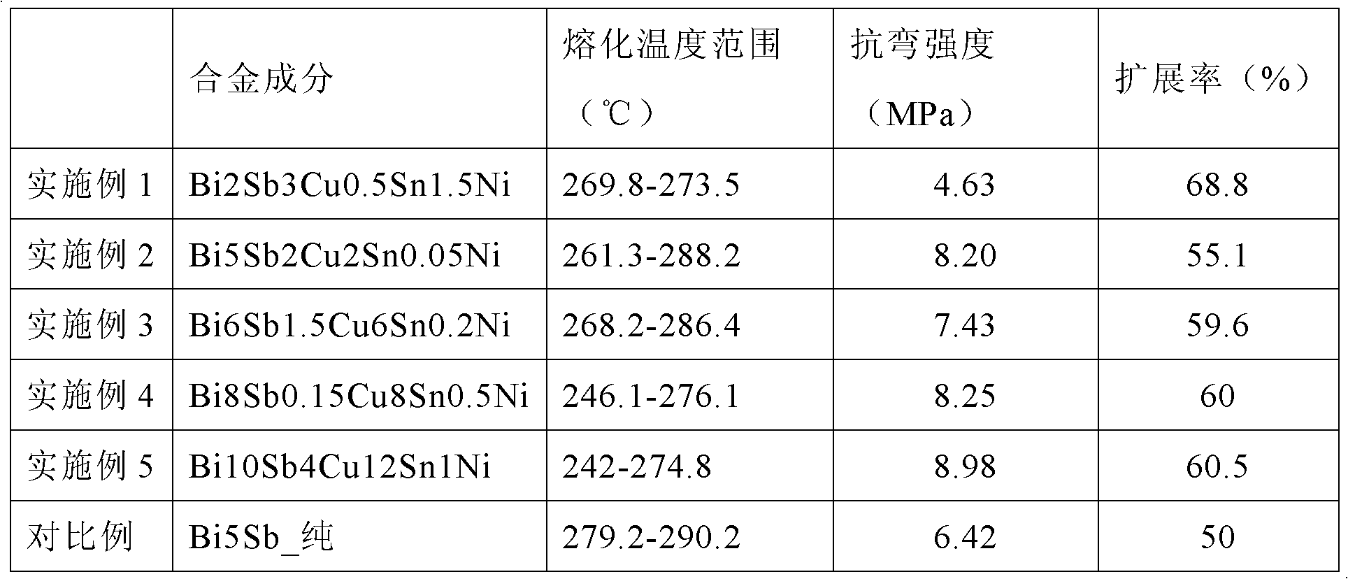
[0024] Mix the raw materials according to the following weight percentages: Sb 2%, Cu 3%, Sn 0.5%, Ni 1.5%, Ga, P and mixed rare earth 0.05%, the balance being Bi, and put them in a vacuum melting furnace at 850-1100℃ Keep the temperature for 1-2h, in order to ensure the uniformity of the alloy structure, fully stir and cast and solidify to obtain the brazing alloy. Compared with the comparative example, the melting point is lowered and the spreading performance is improved.

Embodiment 2

[0026] The raw materials are mixed according to the following weight percentages: Sb 5%, Cu 2%, Sn 2%, Ni 0.05%, Ga, P and mixed rare earth 0.01%, and the balance is Bi. Put them in a vacuum melting furnace at 850-1100°C. 1-2h, in order to ensure the uniformity of the alloy structure, fully stir and cast and solidify to obtain the solder alloy before being discharged. Compared with the comparative example, the melting point is lowered, and the spreading performance and mechanical properties are improved.

Embodiment 3

[0028] The raw materials are proportioned according to the following weight percentages: Sb 6%, Cu 1.5%, Sn 6%, Ni 0.2%, Ga, P and mixed rare earth 0.08%, the balance is Bi, and put them in a vacuum melting furnace at 850-1100℃ Keep the temperature for 1-2h, in order to ensure the uniformity of the alloy structure, fully stir and cast and solidify to obtain the brazing alloy. Compared with the comparative example, the melting point is lowered, and the spreading performance and mechanical properties are improved.


PUM


Abstract

The invention relates to Pb-free solder for high-temperature electronic packaging, which has good wetting properties, mechanical properties and oxidation resistance and high welding strength. The Pb-free solder comprises 1-12% by weight of Sb, 0.01-5% by weight of Cu, 0-15% by weight of Sn, 0.01-2% by weight of Ni, 0-0.1% by weight of X and the balance of Bi, wherein the X is one or more of the Ga, P and mixed rare earth. The Pb-free solder disclosed by the invention is suitable for electronic packaging.

Description

Technical field [0001] The invention relates to a high-temperature electronic packaging lead-free solder and its preparation technology, which is particularly suitable for soldering in the field of electronics and microelectronic packaging, and also applicable to the field of soldering requiring joint filling and fastening. Background technique [0002] High-lead solder (Pb content higher than 85wt.%) is widely used in the high temperature field of microelectronic packaging. High-lead solder not only provides a stable and reliable connection for microelectronic components working in a hot environment, but also is often used as a high melting point alloy during step soldering for the first-level packaging of electronic components. High-lead solder is also a large-scale IT equipment And network infrastructure, high-power power supplies and switches, automotive electronics, aerospace and other military and civil fields such as critical electronic component packaging are extremely im...

Claims


Application Information

Patent Timeline
IPC IPC(8): B23K35/26C22C1/02
Inventor 刘平杨倡进顾小龙胡兰伟崔良
Owner ZHEJIANG ASIA GENERAL SOLDERING & BRAZING MATERIAL
Learn More