Silicon through hole etching method

A technology of through-silicon via and etching machine, applied in coating, microstructure device, microstructure technology and other directions, can solve the problems of substrate sidewall corrugation, metal pollution, easy damage of photoresist, etc., to eliminate sidewall corrugation , Easy to remove, avoid metal pollution effect

Inactive Publication Date: 2012-05-02
HUAZHONG UNIV OF SCI & TECH
View PDF6 Cites 15 Cited by
  • Summary
  • Abstract
  • Description
  • Claims
  • Application Information

AI Technical Summary

Problems solved by technology

[0004] The invention provides a through-silicon via etching method, which solves the problems of corrugation on the side wall of the substrate, easy damage of photoresist and metal contamination in deep silicon etching using the existing Bosch process and metal mask.

Method used


Image

  • Silicon through hole etching method
  • Silicon through hole etching method
  • Silicon through hole etching method

Examples


Embodiment 1

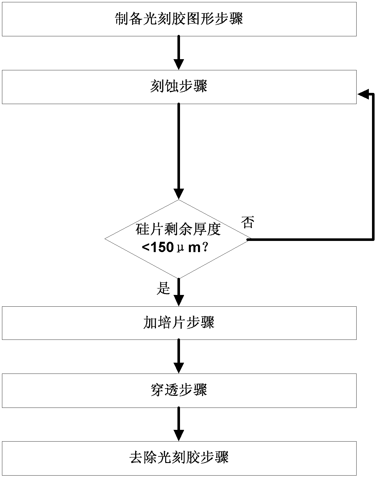
[0026] Embodiment 1, comprising:

[0027] (1) Steps for preparing graphics:

[0028] Uniformly coat photoresist on a 4-inch silicon wafer with a thickness of 200 μm, and the thickness of the photoresist is 10 μm; use a photolithography process and a karl suss MA6 photolithography machine to prepare the required pattern on the photoresist;

[0029] (2) Etching steps:

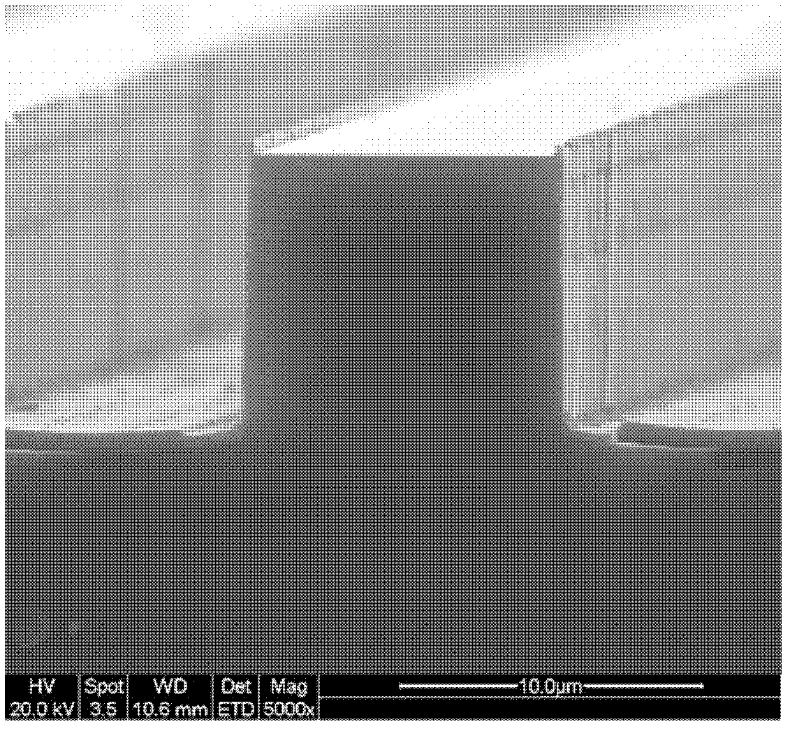
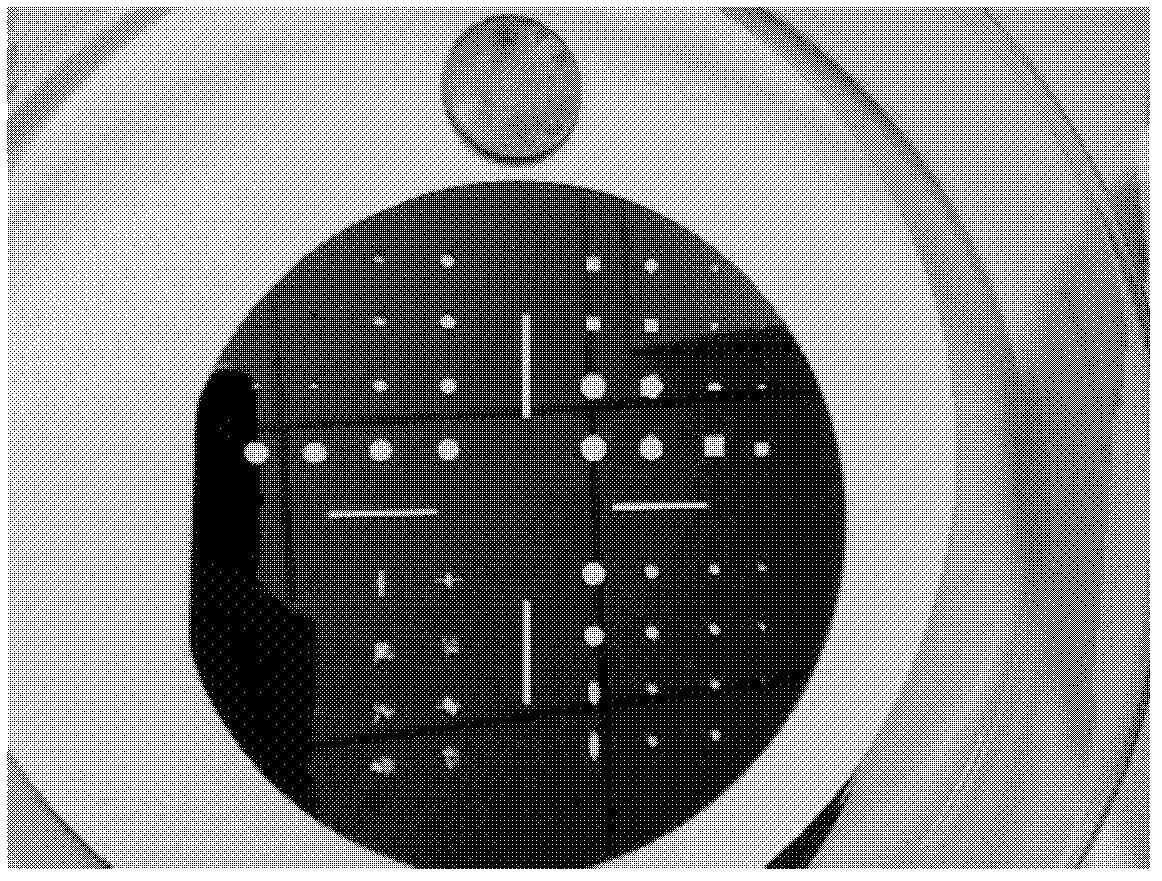
[0030] Using the Bosch process, in the Oxford Plasmalab ICP inductively coupled plasma etching machine of Oxford Instruments, after 50 alternate etching and passivation processes on the silicon wafers prepared for the pattern, the processing is suspended, and the photoresist is cooled. 50 times of etching and passivation alternate processing; this cycle alternates until the remaining thickness of the etched part of the silicon wafer is less than 150um; the verticality and smoothness of the etched side wall are as follows figure 2 Shown; process chamber pressure of inductively coupled plasma etching machine: 40...

Embodiment 2

[0040] Embodiment 2, comprising:

[0041] (1) Preparation of photoresist pattern steps:

[0042] Evenly coat photoresist on a 2-inch silicon wafer with a thickness of 250 μm, and the thickness of the photoresist is 15 μm; use photolithography to prepare the required pattern on the photoresist;

[0043] (2) Etching steps:

[0044] Using the Bosch process, in the Oxford Plasmalab ICP inductively coupled plasma etching machine of Oxford Instruments, after 40 alternate etching and passivation processes on the silicon wafers prepared for the pattern, the processing was suspended, and after the photoresist cooled, another 40 times were performed. The secondary etching and passivation are alternately processed; this cycle alternates until the remaining thickness of the etched part of the silicon wafer is less than 150um; the process chamber pressure of the inductively coupled plasma etching machine: 40mtorr, the temperature: 10°C;

[0045] In each alternate process of etching and p...

Embodiment 3

[0054] Embodiment 3, comprising:

[0055] (1) Preparation of photoresist pattern steps:

[0056] Uniformly coat photoresist on a 4-inch silicon wafer with a thickness of 250 μm, and the thickness of the photoresist is 15 μm; use a photolithography process and a karl suss MA6 photolithography machine to prepare the required pattern on the photoresist;

[0057] (2) Etching steps:

[0058] Using the Bosch process, in the Oxford Plasmalab ICP inductively coupled plasma etching machine of Oxford Instruments, after 80 times of etching and passivation alternately processed the patterned silicon wafer, the processing was suspended, and after the photoresist cooled down, another 80 times were performed. The secondary etching and passivation are alternately processed; this cycle alternates until the remaining thickness of the etched part of the silicon wafer is less than 150um; the verticality and smoothness of the etched sidewall are as follows figure 2 Shown; process chamber pressu...


PUM


Abstract

The invention provides a silicon through hole etching method and belongs to the field of micro nano machining of micro electro mechanical systems, and the method can be used for solving the problems that the side wall of a substrate generates ripples, a photoresist can be easily damaged and metal pollution is caused when an existing Bosch process and a metal mask are utilized to carry out deep silicon etching. The method provided by the invention comprises a pattern preparation step, an etching step, a culture slice adding step, a penetrating step and a photoresist removing step. In the etching step, processing is stopped after circulative and alternative etching is finished, so that the photoresist is cooled and the protective action of the photoresist is prevented from being reduced; then circulative etching is carried out again; passivating gas is added into etching gas; and the etching gas is added into the passivating gas for improving the smoothness of the side wall. In the culture slice adding step, a silicon wafer is adhered to the upper surface of a culture slice,thus preventing silicon wafer fracture and equipment damage after etching penetration. The method provided by the invention has the advantages that the process is simple and the etching speed is quick; the photoresist utilized as the mask can be easily removed after being etched, and metal pollution is avoided; the verticality of the side wall of a through hole is easily controlled; the smoothness of the side wall is improved; and the ripples on the side wall are eliminated.

Description

technical field [0001] The invention belongs to the field of micro-nano processing of micro-electro-mechanical systems (MEMS), and in particular relates to a through-silicon hole etching method. Background technique [0002] In recent years, computers, communications, automotive electronics, aerospace industry and other consumer products have put forward higher requirements for microelectronic packaging, that is, smaller, thinner, lighter, high reliability, multi-function, low power consumption and low Cost, it is necessary to make many vertical interconnection vias on the silicon wafer to realize the electrical interconnection between different chips, so the through-silicon via etching process has become an important technology in the field of micro-electromechanical system (MEMS) micro-nano processing. [0003] The through-silicon via etching process is a deep silicon etching process using plasma dry etching. At present, the deep silicon etching generally uses Bosch proces...

Claims


Application Information

Patent Timeline
Patent Type & Authority Applications(China)
IPC IPC(8): B81C1/00
Inventor 廖广兰高阳史铁林谭先华李晓平卓锐
Owner HUAZHONG UNIV OF SCI & TECH
Why Eureka
Try Eureka