Manufacturing method of mechanical uniaxial strain SOI (silicon-on-insulator) wafer

A technology of uniaxial strain and manufacturing method, which is applied in semiconductor/solid-state device manufacturing, electrical components, circuits, etc., can solve the problems of silicon wafers being easily broken, complicated process steps, and long manufacturing cycle, and achieve small surface roughness , good strain effect and high yield

Inactive Publication Date: 2012-05-02
XIDIAN UNIV
View PDF1 Cites 7 Cited by
  • Summary
  • Abstract
  • Description
  • Claims
  • Application Information

AI Technical Summary

Problems solved by technology

[0011] Compared with the present invention, this method has the following main disadvantages: 1) process steps are complicated: the method must experience thermal oxidation, H + Ion implantation, stripping annealing and other essential processes and related steps
3) Long production cycle: additional thermal oxidation, H + Process steps such as ion implantation and stripping annealing increase the time of its fabrication
4) Low yield: This method is to use two overlapping silicon wafers for mechanical bending and bonding, and to perform high-temperature peeling in the bent state, and the silicon wafers are easily broken

Method used


Image

  • Manufacturing method of mechanical uniaxial strain SOI (silicon-on-insulator) wafer
  • Manufacturing method of mechanical uniaxial strain SOI (silicon-on-insulator) wafer
  • Manufacturing method of mechanical uniaxial strain SOI (silicon-on-insulator) wafer

Examples


Embodiment 1

[0039] Embodiment 1: Preparation of 4-inch uniaxially strained SOI wafer

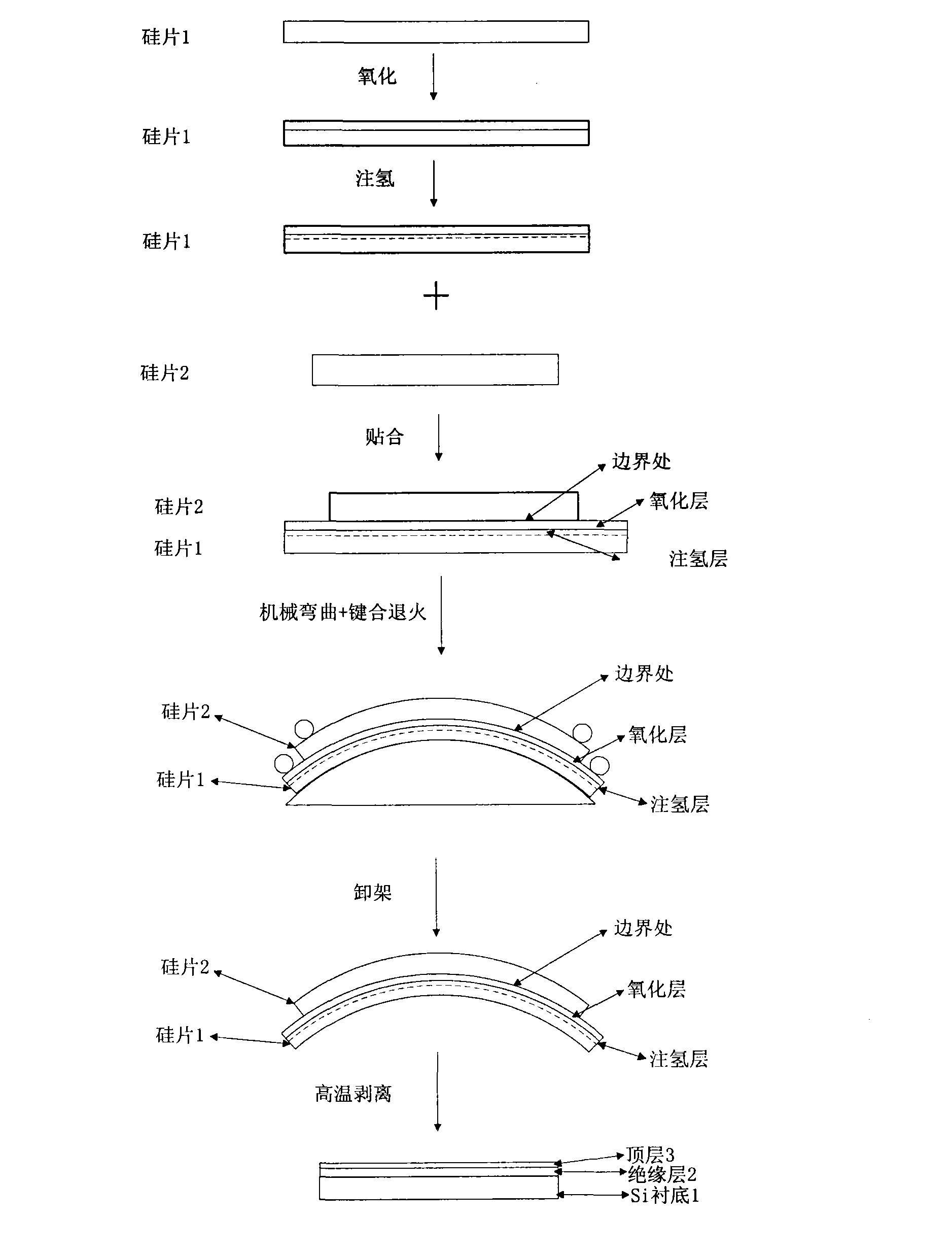
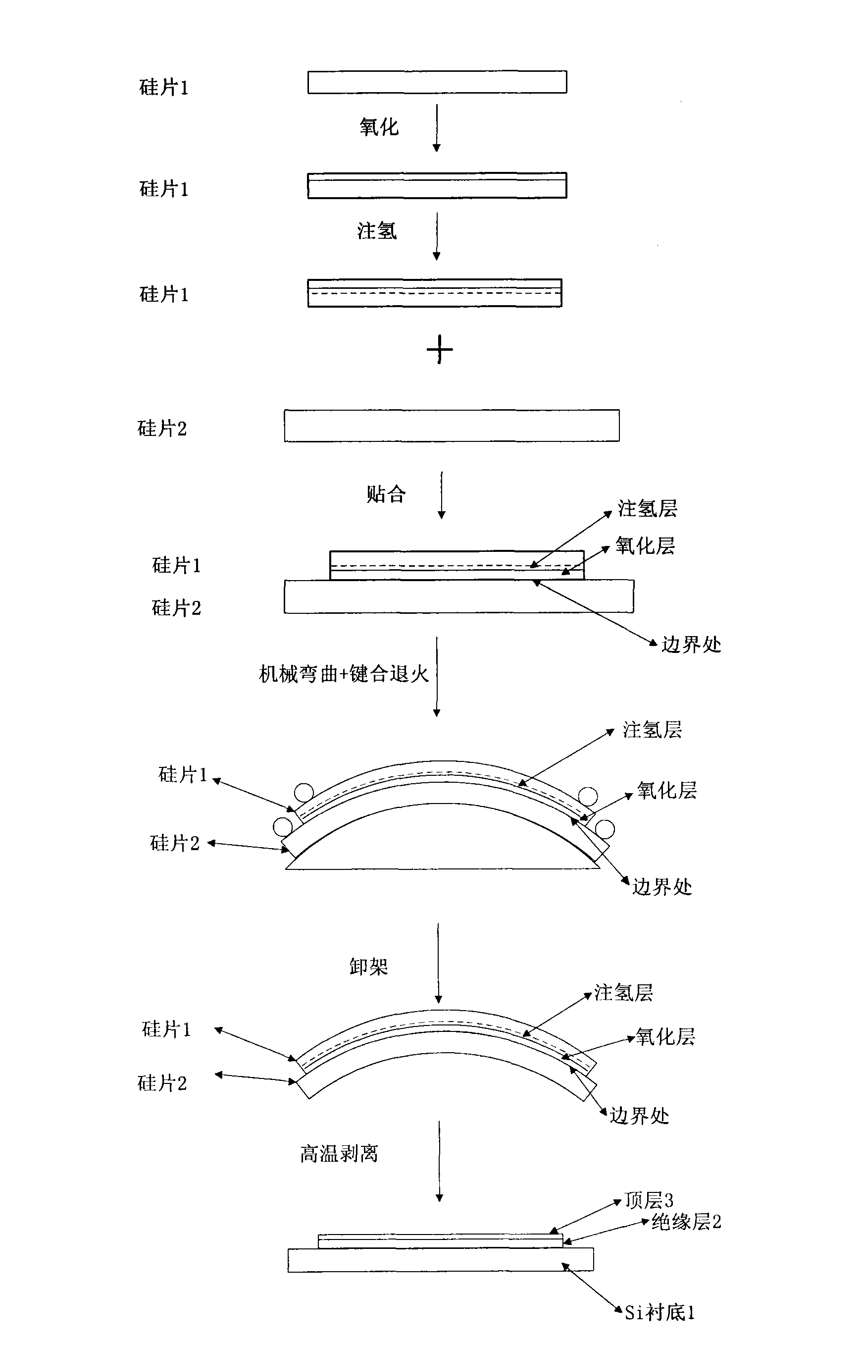
[0040] 1. SOI wafer selection: 4-inch (100) or (11O) wafer ((100) or (110) refers to a certain crystal surface of the SOI wafer crystal surface), Si substrate thickness 0.4mm, SiO 2 The thickness of the buried insulating layer is 500nm, and the thickness of the top layer Si is 500nm.

[0041] SOI wafer diameter selection: The larger the diameter of the SOI wafer, the smaller the minimum bending radius of the bend, and the greater the strain of the obtained uniaxially strained SOI wafer, and the electron migration of the final uniaxially strained SOI wafer The enhancement of rate and hole mobility is also higher. For the SiO-based 2 For uniaxially strained SOI wafers with buried insulating layers, SOI wafers with different diameters from 3 inches to 16 inches can be selected according to the different processes of SOI devices and circuits.

[0042] SOI wafer crystal face and crystal orientation selec...

Embodiment 2

[0060] Embodiment 2: Preparation of 6-inch uniaxially strained SOI wafer

[0061] 1. SOI wafer selection: 6-inch (100) or (110) crystal plane, Si substrate thickness 0.55mm, SiO 2 The buried insulating layer is 300nm thick, and the top Si layer is 50nm thick.

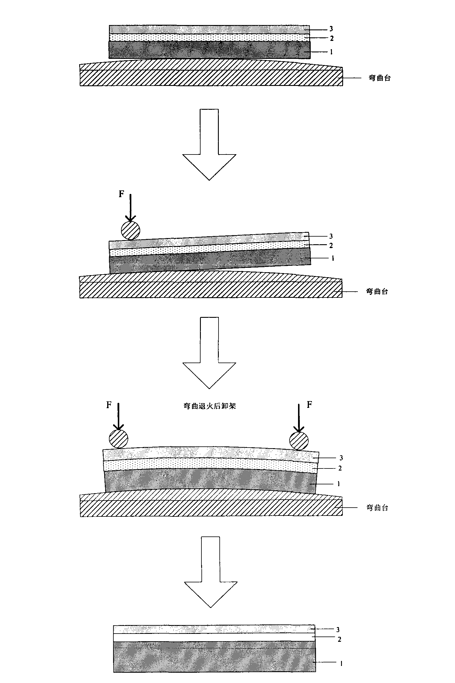
[0062] 2. Selection of bending radius of curvature: According to the selected SOI wafer, the radius of curvature of the bending table is selected to be 0.75m.

[0063] 3. SOI wafer bending process steps:

[0064] 1) Place the top Si side of the SOI wafer on a clean bending table with its or direction parallel to the bending direction, such as image 3 or Figure 4 shown;

[0065] 2) Two cylindrical horizontal pressure bars on the bending table are placed horizontally at both ends of the SOI wafer, 1 cm away from its edge;

[0066] 3) Rotate the ejector nut of one of the pressure rods on the bending table to fix one end of the SOI wafer first;

[0067] 4) Slowly turn the ejector nut of another pressing rod to gra...

Embodiment 3

[0075] Embodiment 3: Preparation of 8-inch uniaxially strained SOI wafer

[0076] 1. SOI wafer selection: 8-inch (100) or (110) crystal plane, Si substrate thickness 0.68mm, SiO 2 The buried insulating layer is 1000nm thick, and the top Si layer is 1000nm thick.

[0077] 2. Selection of bending radius of curvature: According to the selected SOI wafer, the radius of curvature of the bending table is selected to be 0.5m.

[0078] 3. SOI wafer bending process steps:

[0079] 1) Place the Si layer on the top layer of the SOI wafer upwards (or downwards) on an arc-shaped bending table, and its bending direction is parallel to the or direction, such as image 3 or Figure 4 shown;

[0080] 2) Two cylindrical horizontal pressure bars on the bending table are placed horizontally at both ends of the SOI wafer, 1 cm away from its edge;

[0081] 3) Rotate the ejector nut of one of the pressure rods on the bending table to fix one end of the SOI wafer first;

[0082] 4) Slowly tur...


PUM

PropertyMeasurementUnit
Thicknessaaaaaaaaaa
Thicknessaaaaaaaaaa
Bending radiusaaaaaaaaaa

Abstract

The invention discloses a manufacturing method of a mechanical uniaxial strain SOI (silicon-on-insulator) wafer. The method comprises the following steps: 1) putting an SOI wafer on a cambered bending table, wherein the top layer (Si layer surface) of the SOI wafer faces up or down; 2) respectively horizontally putting two cylindrical stainless steel pressure bars on both ends of the SOI wafer, wherein the two cylindrical stainless steel pressure bars are respectively 1cm away from the edge of the SOI wafer; 3) slowly rotating a screw cap which connects the pressure bars, so that the SOI wafer is gradually bent along the cambered table until the SOI wafer is completely laminated on the cambered table; 4) putting the cambered bending table carrying the SOI wafer in an annealing furnace, and carrying out annealing; 5) after the annealing finishes, slowly cooling to room temperature, and taking out the cambered bending table carrying the SOI wafer; and 6) rotating the screw cap which connects the pressure bars, and slowly elevating the pressure bars until the bent SOI wafer restores to the original state. The invention has the advantages of 1) favorable strain effect, 2) small surface roughness, 3) fewer surface defects, 4) favorable thermal properties, 5) high electric properties, 6) high yield, 7) wide annealing temperature range, 8) simple manufacturing technique, 9) fewer manufacturing devices which can be self-made, 10) low manufacturing cost and 11) accessible raw materials.

Description

technical field [0001] The invention belongs to the technical field of microelectronics, and relates to a semiconductor substrate material manufacturing process technology, specifically a method for manufacturing a uniaxial strain SOI (Silicon On Insulator, silicon on an insulating layer) wafer, which can be used for making ultra-high speed, low SOI wafers required for power consumption, radiation-resistant semiconductor devices and integrated circuits can significantly improve the electron mobility and hole mobility of traditional SOI wafers, and overcome the high-field degradation of traditional biaxial strain SOI mobility enhancement. Compared with the existing uniaxial strain SOI technology, the invention has the advantages of high strain degree, simple process, high yield and low cost. Background technique [0002] Compared with bulk Si technology, SOI technology has the advantages of high speed, low power consumption, high integration density, small parasitic capacitan...

Claims


Application Information

Patent Timeline
IPC IPC(8): H01L21/762
Inventor 戴显英张鹤鸣郝跃王琳宁静李志王晓晨查冬付毅初
Owner XIDIAN UNIV
Why Eureka
Try Eureka