Process for production of semiconductor light-emitting element substrate

A technology of light-emitting elements and manufacturing methods, applied in semiconductor/solid-state device manufacturing, semiconductor devices, optical elements, etc.

Active Publication Date: 2012-05-02
SHINCRON KK
View PDF3 Cites 3 Cited by
  • Summary
  • Abstract
  • Description
  • Claims
  • Application Information

AI Technical Summary

Problems solved by technology

[0022] However, the technique disclosed in Patent Document 2 is a technique aimed at forming a film on a substrate made of a material having a low heat distortion temperature such as plastic by a vacuum evaporation method. More specifically, it is a technique for manufacturing a semiconductor optical element. The technique for forming a high-performance reflective layer is not described

Method used


Image

  • Process for production of semiconductor light-emitting element substrate
  • Process for production of semiconductor light-emitting element substrate
  • Process for production of semiconductor light-emitting element substrate

Examples


Embodiment Construction

[0105] Hereinafter, an embodiment of the present invention will be described with reference to the drawings. In addition, the components, configurations, etc. described below do not limit the present invention, and it is obvious that various changes can be made in accordance with the gist of the present invention.

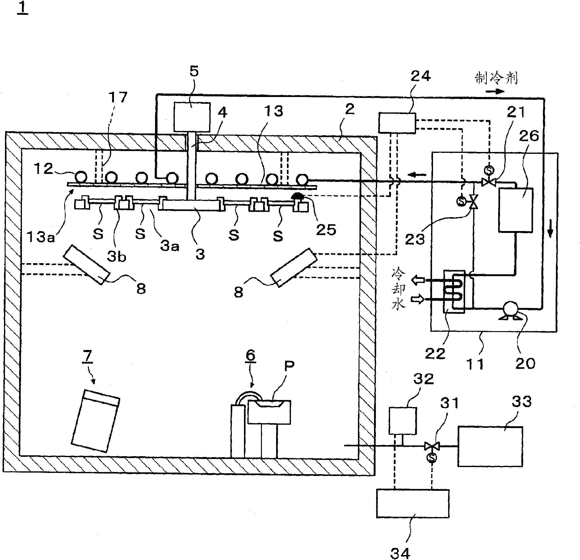
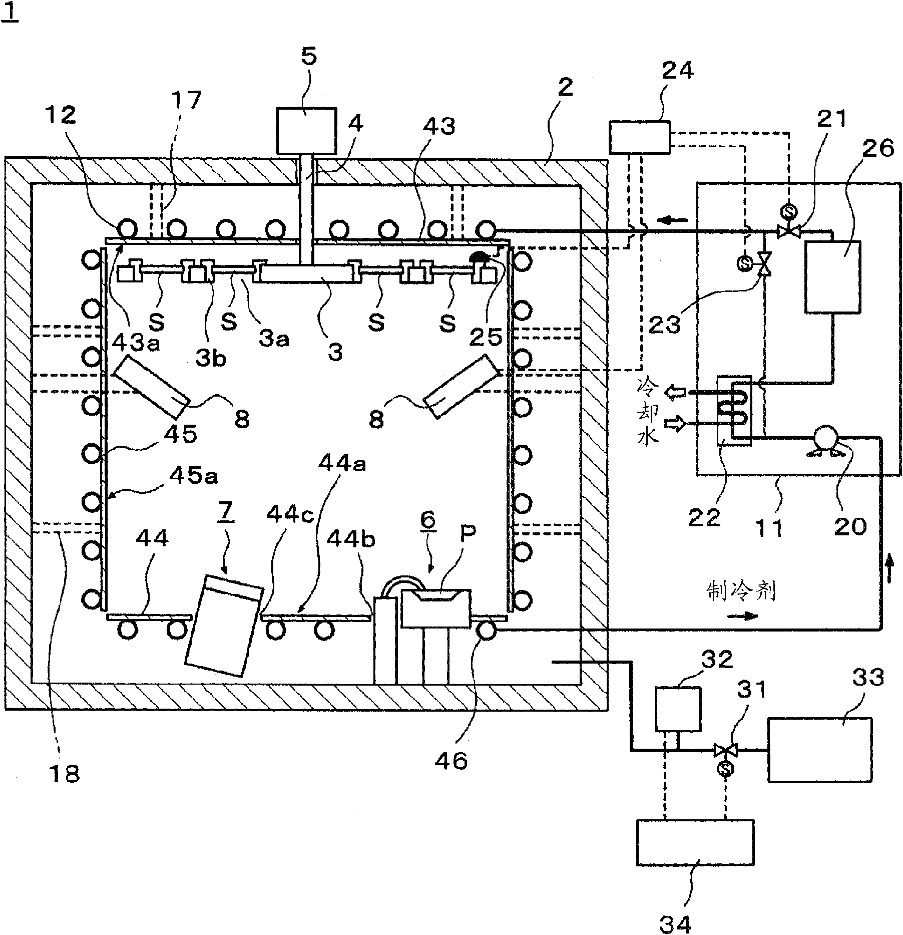
[0106] figure 1 It is an explanatory diagram of an ion-assisted vapor deposition apparatus 1 as a thin film forming apparatus, and a part of the apparatus is shown in cross section.

[0107] As shown in the figure, the ion-assisted vapor deposition apparatus 1 includes as main components: a vacuum chamber 2, a substrate holder 3, a substrate holder rotating shaft 4, a substrate holder rotating motor 5, an evaporation source 6, an ion source 7, a heating unit 8, Refrigerator 11, refrigerant pipe 12 and cooling plate 13.

[0108] The vacuum chamber 2 is a container for film formation inside. The vacuum chamber 2 of the present embodiment is a hollow body having a substan...


PUM

PropertyMeasurementUnit
refractive indexaaaaaaaaaa

Abstract

Disclosed is a process for producing a high-performance semiconductor light-emitting element substrate, which has a reduced production time. Specifically disclosed is a process for producing a semiconductor light-emitting element substrate, which is characterized by comprising: a substrate heating step (S3) of heating a substrate; a substrate washing step (S6) of washing the substrate (S); a dielectric material layer formation step (S7) of depositing dielectric material layers (H, L) on the substrate (S); a substrate heating termination step (S8) of terminating the heating of the substrate; a cooling step (S9) of absorbing a radiation heat by means of cooling means (11, 12, 13) to cool the substrate (S) and a substrate supporting means (3); and a reflective layer formation step (S11) of depositing a reflective layer (R) on the dielectric material layers (H, L).

Description

Technical field [0001] The present invention relates to a method for manufacturing a semiconductor light-emitting element substrate, and more particularly to a method for manufacturing a high-performance semiconductor light-emitting element substrate by shortening the manufacturing time. Background technique [0002] Semiconductor light-emitting elements (LEDs) are practically used as light sources because of their low power consumption, long life, and high luminous efficiency. And in the field of semiconductor light-emitting elements, GaN-based compound semiconductors such as GaN, GaAlN, and InGaN are widely used in visible light-emitting devices and high-temperature operation electronic devices. [0003] In the production of GaN-based compound semiconductors, in order to grow a semiconductor film on the surface of a substrate, a sapphire substrate is generally used as a crystal substrate. Since the sapphire substrate is insulating, it is not possible to provide an electrode on t...

Claims


Application Information

Patent Timeline
Patent Type & Authority Applications(China)
IPC IPC(8): C23C14/24G02B1/10H01L33/60C23C14/06H01L21/304H01L33/46
CPCG02B5/0858C23C14/32C23C14/505C23C14/54H01L2933/0025H01L33/46C23C14/541H01L33/02
Inventor 松本繁治橘孝彦
Owner SHINCRON KK
Why Eureka
Try Eureka