Method for preparing nano-gap electrodes on surface of nano-pore and in nano-pore

A nano-gap electrode and nano-gap technology, applied in the direction of nanotechnology, nanotechnology, nanotechnology for sensing, etc., can solve the problem of not being able to reach a single nucleotide, and achieve the effect of improving accuracy

Inactive Publication Date: 2012-05-09
SOUTHEAST UNIV
View PDF1 Cites 27 Cited by
  • Summary
  • Abstract
  • Description
  • Claims
  • Application Information

AI Technical Summary

Problems solved by technology

[0004] However, due to the limitations of the stability and insulation of the current preparation materials, processing technology, and nano-engraving technology, the length of the current solid-state nanopore cannot reach the length of a single nucleotide (<0.4nm), so a chain passing through the nanometer During the pore process, multiple nucleotides will be blocked in the pore at the same time to cause changes in the current. Due to these factors, it is temporarily impossible to simply rely on the detection of changes in the longitudinal blocking current to achieve single-base sequencing of DNA.

Method used


Image

  • Method for preparing nano-gap electrodes on surface of nano-pore and in nano-pore
  • Method for preparing nano-gap electrodes on surface of nano-pore and in nano-pore
  • Method for preparing nano-gap electrodes on surface of nano-pore and in nano-pore

Examples


Embodiment 1

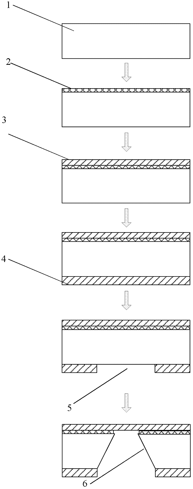
[0030]On the front silicon nitride film, the desired metal line pattern is formed on the photoresist by ultraviolet lithography, and then the metal line pattern 7 is evaporated using an electron beam evaporation apparatus. Finally, at the position of the metal wire of the etching window, a nano-gap 8 is etched on the metal wire by using focused electron beam etching, and then a nano-hole 9 is etched to form a surface nano-gap electrode at the opening of the nano-hole.

Embodiment 2

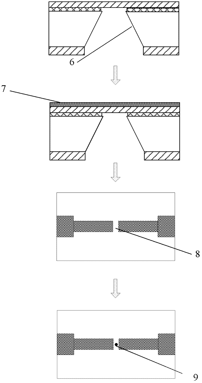
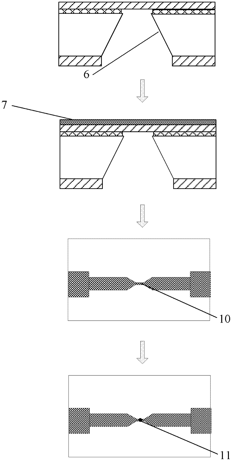
[0032] On the front silicon nitride film, the desired metal line pattern is formed on the photoresist by ultraviolet lithography, and then the metal line pattern 7 is evaporated using an electron beam evaporation apparatus. Finally, at the position of the metal wire in the etching window, use a focused electron beam to etch a metal wire with a line width of microns into a nanowire 10, and then use a focused ion beam or a high-energy electron beam to etch a nanometer-sized hole 11 , the metal nanowire is etched just to form a surface nano-gap electrode at the nanohole orifice. The surface nano-gap electrodes prepared by this method can control the spacing within the range of 10-50nm. The spacing of the nano-gap electrodes formed by this method of just etching off the nano-metal wires when etching the nano-pores will be slightly larger than the aperture of the nano-pores. image 3 The picture is too small to show it in detail.

Embodiment 3

[0034] On the basis of Example 2, the Pt lines are deposited on the surface of the nanogap electrode 12 by using the focused ion beam induced deposition method. The width of the Pt line is set between 5-50nm, the length depends on the distance from the nano-electrode etched by FIB to the edge of the nano-hole, and the thickness is between a few nanometers and tens of nanometers. Select an accelerating voltage of 30kV, select different ion beams to deposit Pt lines, first select one of the electrodes to induce the deposition of Pt lines 13 on one side, stop deposition when the Pt line is close to the edge of the hole, and then start from the other electrode Deposit the Pt line 14 on the other side, and stop the deposition when the Pt line is close to the edge of the hole, and finally form a nanogap electrode with a spacing of 1-10 nm above the nanohole.


PUM

PropertyMeasurementUnit
widthaaaaaaaaaa

Abstract

The invention relates to a method for preparing nano-gap electrodes on the surface of a nano-pore and in the nano-pore. The method enables two-dimensional two-channel simultaneous detection of signal changes in a molecular through hole to be realized and accuracy of sequencing of a nano-pore to be improved. The method for preparing a nano-gap electrode on the surface of a nano-pore comprises the following steps: forming a micron-sized metal line on the surface of a substrate, etching the micron-sized metal line into a metal line with line width at a nanometer level, etching a through nano-pore in the substrate at a position corresponding to the nanometer metal line, and cutting the metal line through corrosion so as to directly form a surface nano-gap electrode at the opening of the nano-pore. To improve the invention, a micron-sized metal line is formed on the surface of the substrate and etched until the line width of the metal line is 10 to 50 nm, then etching is carried out on themetal line so as to form opposite electrodes, a through nano-pore is etched in the substrate at a position corresponding to a nano-gap, the metal line is allowed to grow towards the edge of the nano-pore, and therefore, a surface nano-gap electrode is formed at the opening of the nano-pore.

Description

technical field [0001] The invention relates to a method for preparing nano-gap electrodes on the surface of nano-holes and inside the holes. Background technique [0002] Nanopores are used in the detection of biomolecules through electrophoresis to drive a biomolecule through a small hole with a diameter of several nanometers. In 1996, Kasianowicz and his colleagues reported for the first time that single-stranded DNA or RNA passed through the α-hemolysin nanopore self-assembled on the lipid bilayer under the action of an electric field, and changed the conductance of the nanopore when the DNA molecule passed through the pore, The current changes, resulting in the phenomenon of blocking current (blockade current). Since different bases have different atomic compositions, they will generate different blocking currents when passing through the nanopore. According to the detectable signal, four different bases A, T, C, and G can be distinguished. Thereby obtained the sequen...

Claims


Application Information

Patent Timeline
Patent Type & Authority Applications(China)
IPC IPC(8): G01N27/30B82Y40/00B82Y15/00
Inventor 叶晓峰刘丽萍吴宏文孔婧琳陆祖宏刘全俊易红
Owner SOUTHEAST UNIV
Why Eureka
Try Eureka