Method for crystallizing noncrystalline silicon by induction heating

A technology of induction heating and amorphous silicon, applied in the direction of induction heating, induction heating devices, chemical instruments and methods, etc., can solve the problems of uneven crystallization, high price and maintenance costs, poor stability, etc., and achieve the goal of induction heating equipment Simple, high energy efficiency utilization, high heating efficiency effect

Inactive Publication Date: 2012-05-23
INESA ELECTRON
View PDF0 Cites 16 Cited by
  • Summary
  • Abstract
  • Description
  • Claims
  • Application Information

AI Technical Summary

Problems solved by technology

[0002] Thin-film transistors are widely used in display devices. At present, the mainstream technology of thin-film transistors is amorphous silicon thin-film transistor technology, but amorphous silicon thin-film transistors have problems of low mobility and poor stability, which cannot be applied to some high-demand fields, such as Organic light-emitting display devices, polysilicon thin film transistors can solve the above problems, so people began to apply polysilicon thin film transistor technology in organic light emitting display devices, polysilicon thin film transistor technology can solve the above problems
The crystallization technology of amorphous silicon thin film is the most critical in the manufacturing technology of polysilicon thin film transistors. In order to crystallize on the glass substrate, low temperature crystallization technology must be used. At present, the main low temperature crystallization technology is laser annealing, but laser annealing There are still some limitations in the technology. For example, the unstable power of the excimer laser will cause the inhomogeneity of crystallization, which will lead to the inhomogeneity of the displayed image. Although the power of the semiconductor laser is stable, the power of the semiconductor laser is relatively small at present, and The wavelength of semiconductor lasers and the absorption wavelength of silicon are difficult to match
In addition, the laser annealing equipment is complicated, it is difficult to expand the large size, and the price and maintenance costs are very high

Method used


Image

  • Method for crystallizing noncrystalline silicon by induction heating
  • Method for crystallizing noncrystalline silicon by induction heating

Examples


Embodiment Construction

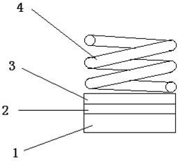
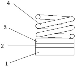
[0009] Such as figure 1 As shown in the schematic diagram of induction heating amorphous silicon crystallization, first deposit a layer of amorphous silicon film 2 on the glass substrate 1, then cover the amorphous silicon film 2 with a layer of metal film 3, and put the opening end of the induction coil 4 close to the metal The induction coil is connected to the induction power supply, and a strong alternating current is passed through the induction coil, which can reach thousands of amperes. A strong alternating magnetic field is generated in the coil, and the alternating magnetic field is perpendicular to the metal film and the amorphous silicon film 2, and the metal film 3 will generate The strong induced eddy current can rapidly heat the metal film 3, thereby heating the amorphous silicon film 2 covered under the metal film 3. After the amorphous silicon is heated, the conductivity is enhanced, and an eddy current is also generated in the alternating magnetic field. Furth...


PUM

PropertyMeasurementUnit
thicknessaaaaaaaaaa
thicknessaaaaaaaaaa
thicknessaaaaaaaaaa

Abstract

The invention relates to a method for crystallizing noncrystalline silicon by induction heating, wherein a strong alternating magnetic field is generated by using an induction coil, the alternating magnetic field approaches a noncrystalline silicon thin film covered with a metal film, the metal film can generate strong induction vortex current which is capable of rapidly heating the metal film so as to heat the noncrystalline silicon under the metal film, the conductivity of the heated noncrystalline silicon is enhanced, a vortex current can be also generated in the alternating magnetic field to further heat the alternating magnetic field per se, and therefore the noncrystalline silicon thin film is rapidly heated to reach the crystallization temperature, and the purpose of crystallization is achieved; and the method disclosed by the invention has the advantages of simple required equipment and low cost and is beneficial to popularization and application of polysilicon thin film transistors.

Description

technical field [0001] The invention relates to an electronic display device, in particular to an induction heating amorphous silicon crystallization method. Background technique [0002] Thin-film transistors are widely used in display devices. At present, the mainstream technology of thin-film transistors is amorphous silicon thin-film transistor technology, but amorphous silicon thin-film transistors have problems of low mobility and poor stability, which cannot be applied to some high-demand fields, such as Organic light emitting display devices, polysilicon thin film transistors can solve the above problems, so people start to apply polysilicon thin film transistor technology in organic light emitting display devices, polysilicon thin film transistor technology can solve the above problems. The crystallization technology of amorphous silicon thin film is the most critical in the manufacturing technology of polysilicon thin film transistors. In order to crystallize on th...

Claims


Application Information

Patent Timeline
Patent Type & Authority Applications(China)
IPC IPC(8): C30B28/02H05B6/10H01L21/02
Inventor 陈科刘红君
Owner INESA ELECTRON
Why Eureka
Try Eureka