Ceramic substrate LED apparatus

A technology of LED devices and ceramic substrates, applied in electrical components, electrical solid devices, circuits, etc., can solve the problems of lagging indoor general lighting market, increase heat dissipation surface area, increase PN junction temperature, etc., reduce volume and weight, and improve luminescence Angle, the effect of increasing reliability

Inactive Publication Date: 2012-05-23
浙江雄邦节能产品有限公司
View PDF10 Cites 7 Cited by
  • Summary
  • Abstract
  • Description
  • Claims
  • Application Information

AI Technical Summary

Problems solved by technology

China has formed certain characteristics in the field of lighting, among which outdoor lighting has developed the fastest. There are hundreds of LED companies and dozens of demonstration roads have been built, but it is still lagging behind in the indoor general lighting market.
[0005] With the evolution of LED technology, single high-power lighting products have gradually become the mainstream. However, with the improvement of LED brightness, the temperature of its medium is also greatly increased. The traditional aluminum substrate must increase the heat dissipation surface area, thus making the overall structure of the LED The increase in weight and volume is not conducive to use
Chinese patent 200920260245.2 discloses a high-radiation ceramic heat dissipation coating on the surface of the substrate (aluminum or copper or magnesium alloy), which mainly uses radiation heat dissipation to cool the LED, which is different from the current main conduction heat dissipation and convection heat dissipation. Compared with it, it has certain advantages, but it is mainly installed on the outer surface of the lampshade or bottom of the LED lamp, and does not fundamentally solve the weakening of the luminous brightness and the attenuation of the service life caused by the high internal temperature of the LED crystal.
[0006] At the same time, the current high-density packaging method of concentrating fluorescent substances on the LED chip further increases the temperature of the PN junction.

Method used


Image

  • Ceramic substrate LED apparatus
  • Ceramic substrate LED apparatus
  • Ceramic substrate LED apparatus

Examples


Embodiment Construction

[0024] The embodiments of the present invention will be described in more detail below in conjunction with the accompanying drawings, so that those skilled in the art can implement them after reading the description.

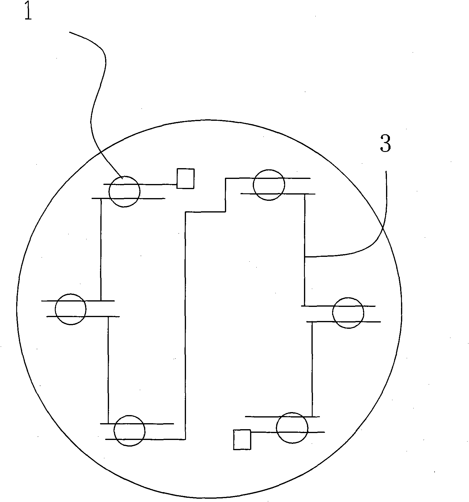
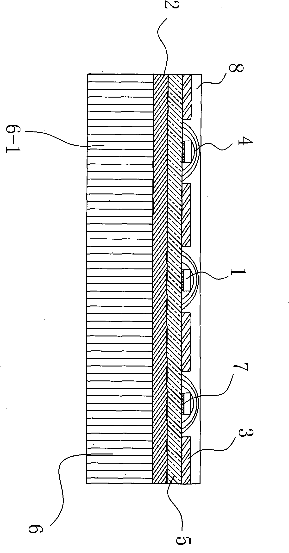
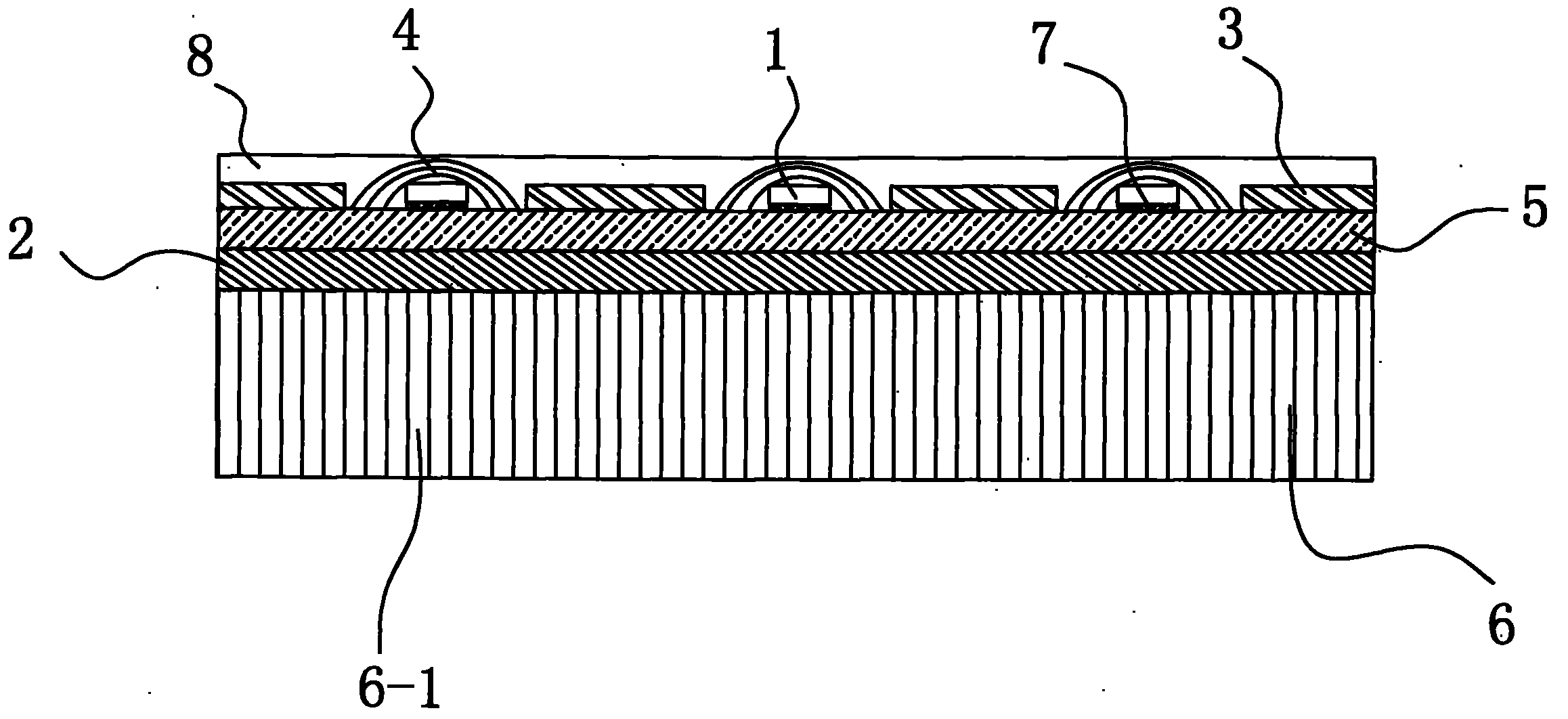
[0025] refer to figure 2 The technical scheme of the present invention includes: LED chip 1, ceramic substrate 6 carrying the chip, circuit layer 3 connected to the LED chip, phosphor powder mixture glue 4 coated on the LED chip, and a bonding layer 7 between the LED chip and the carrying substrate. The ceramic substrate carries the radiation heat dissipation film 2 on one side of the LED and the nano-ceramic glaze coating 5 on the radiation heat dissipation film.

[0026] The phosphor powder mixture glue 4 coated on the LED includes phosphor powder, scattering particles, and silica gel. Phosphor powder mixture 4 is distributed in multiple layers with different concentrations. The density of phosphor powder in the first layer and the second layer adjacent to t...


PUM

PropertyMeasurementUnit
beam angleaaaaaaaaaa

Abstract

The invention discloses a ceramic substrate LED apparatus which comprises an LED wafer, a ceramic substrate which bears the wafer, a circuit layer which is connected with the LED wafer, phosphor mixing glue which is coated on the LED wafer, and a combination layer of the LED wafer and a bearing substrate. The apparatus is characterized by also comprising a radiation heat emission film at one side of the substrate which bears an LED and a nano-ceramic glaze coating layer on the radiation heat emission film. According to the invention, reliability of a product of is raised, heat generated by the LED wafer is rapidly removed, heat emission performance is good, luminous efficacy is high, a service life is long, volume and weight are substantially reduced, a luminescent angle is wide, and a point light source rises to a surface light source.

Description

technical field [0001] The invention relates to the technical field of LED lighting, in particular to a ceramic substrate LED device. Background technique [0002] Under the background of rising global energy shortage concerns, saving energy is an important issue we will face in the future. In the field of lighting, the application of LED light-emitting products is attracting the attention of the world. As a new type of green light source, LED It must be the trend of future development, and the 21st century will enter the era of new lighting sources represented by LEDs. [0003] China's LED industry started in the 1970s. After more than 30 years of development, China's LED industry has initially formed a relatively complete industrial chain including the production of LED epitaxial wafers, the preparation of LED chips, the packaging of LED chips, and the application of LED products. Driven by the "National Semiconductor Lighting Project", seven national semiconductor light...

Claims


Application Information

Patent Timeline
Patent Type & Authority Applications(China)
IPC IPC(8): H01L33/48H01L33/64H01L33/56H01L25/075
Inventor 周超瑛
Owner 浙江雄邦节能产品有限公司
Why Eureka
Try Eureka