Thin film transistor and active matrix rear panel as well as manufacturing methods thereof and display

A technology of thin film transistor and manufacturing method, which is applied in the field of organic light emitting diode display, can solve the problems of low production yield, reduced yield, poor mobility uniformity, etc., and achieves the effects of performance advantages and simple process

Active Publication Date: 2012-05-30
BOE TECH GRP CO LTD
View PDF4 Cites 37 Cited by
  • Summary
  • Abstract
  • Description
  • Claims
  • Application Information

AI Technical Summary

Problems solved by technology

[0006] When AMOLED uses polysilicon TFT as the TFT of the pixel driving circuit, the defects are: high manufacturing cost of laser annealing; poor mobility uniformity caused by polysilicon grain size; low production yield
This pixel drive circuit uses an additional selection signal line to control the isolation TFT, which increases the complexity of the pixel drive circuit design and array design, and may reduce the yield
The low-temperature polysilicon TFT produced by laser annealing and crystallization has relatively poor threshold voltage and mobility uniformity, so a 4T1C pixel drive circuit must be used, which is not conducive to the production of high-resolution displays for bottom-emission AMOLED displays.

Method used


Image

  • Thin film transistor and active matrix rear panel as well as manufacturing methods thereof and display
  • Thin film transistor and active matrix rear panel as well as manufacturing methods thereof and display
  • Thin film transistor and active matrix rear panel as well as manufacturing methods thereof and display

Examples


Embodiment 1

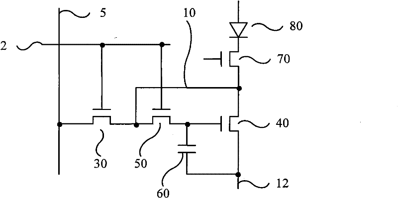
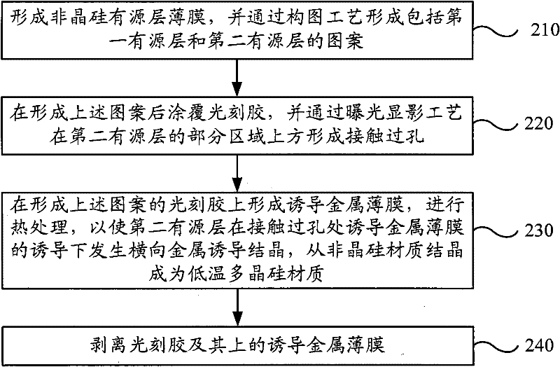
[0074] figure 2 The flow chart of the manufacturing method of the thin film transistor provided by Embodiment 1 of the present invention, the manufacturing method includes the process of preparing the first thin film transistor and the second thin film transistor, wherein the first thin film transistor and the second thin film transistor can be understood as two types Thin film transistors, the number of each type of thin film transistors may be one or more. The first thin film transistor includes a first gate electrode, a first active layer, a first drain electrode, and a first source electrode, and the second thin film transistor includes a second gate electrode, a second active layer, a second drain electrode, and a second source electrode. The structure of the electrode can be in the form of top gate or bottom gate. In the manufacturing method, the process of simultaneously preparing the first active layer and the second active layer specifically includes the following s...

Embodiment 2

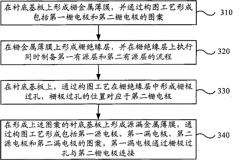
[0091] image 3 The flow chart of the manufacturing method of the thin film transistor provided by the second embodiment of the present invention, this embodiment can be based on the first embodiment, specifically a method for preparing a bottom-gate thin film transistor, then the first thin film transistor and the second thin film transistor are prepared The process of the transistor specifically includes the following steps:

[0092] Step 310, forming a gate metal thin film on the base substrate, and forming a pattern including a first gate electrode and a second gate electrode through a patterning process;

[0093] Step 320, forming a gate insulating layer on the substrate with the above-mentioned structure, and performing the process for simultaneously preparing the first active layer and the second active layer provided in Embodiment 1 on the gate insulating layer;

[0094] Step 330, forming a gate via hole in the gate insulating layer through a patterning process on the...

Embodiment 3

[0098] Figure 4 The flow chart of the manufacturing method of the thin film transistor provided by the third embodiment of the present invention, this embodiment can be based on the first embodiment, specifically a method for preparing a top-gate thin film transistor, then the first thin film transistor and the second thin film transistor are prepared The process of the transistor specifically includes the following steps:

[0099] Step 410, performing the process of simultaneously preparing the first active layer and the second active layer provided by Embodiment 1 on the base substrate;

[0100] Step 420, forming a gate insulating layer on the base substrate with the above pattern formed;

[0101] Step 430, forming a gate metal film on the gate insulating layer, and forming a pattern including the first gate electrode and the second gate electrode through a patterning process;

[0102] Step 440, forming a passivation layer on the base substrate on which the above pattern ...


PUM


Abstract

The invention discloses a thin film transistor and an active matrix rear panel as well as manufacturing methods thereof and a display. The manufacturing method of the thin film transistor comprises a flow of preparing a first thin film transistor and a second thin film transistor, wherein the flow of simultaneously preparing a first active layer and a second active layer comprises the following steps of: forming an amorphous silicon active layer thin film and forming patterns including the first active layer and the second active layer through a pattern forming process; coating photoresist and forming a contact through hole above a partial region of the second active layer through an exposure and development process; forming an inductive metal thin film on the photoresist for forming the pattern and carrying out heat treatment; and then inducing the second active layer by the inductive metal thin film at the contact through hole to be subjected to transverse metal inductive crystallization, so as to crystallize an amorphous silicon material to a low-temperature polycrystalline silicon material; and stripping the photoresist and the inductive metal thin film on the photoresist. According to the invention, through a transverse metal inductive crystallization process, the active layers of the amorphous silicon TFT (Thin Film Transistor) and the low-temperature polycrystalline silicon TFT can be prepared on the same layer at the same time.

Description

technical field [0001] The invention relates to an organic light emitting diode display technology, in particular to a thin film transistor, an active matrix backplane, a manufacturing method thereof and a display. Background technique [0002] Active matrix organic light emitting diode (Active Matrix Organic Light Emitting Diode, referred to as AMOLED) display has active light, high luminous efficiency, high contrast, high resolution, low power consumption, wide color gamut, light, thin, no viewing angle restrictions, and Rich luminescent materials, easy to achieve color display; fast response, high quality dynamic picture; wide temperature range, strong shock resistance; flexible display can be realized; huge space for cost reduction and many other advantages. Therefore, AMOLED has great potential in the current world flat panel display industry. AMOLED display technology has developed rapidly in the past ten years and has achieved major breakthroughs. One of the ways to...

Claims


Application Information

Patent Timeline
Patent Type & Authority Applications(China)
IPC IPC(8): H01L21/77H01L29/786H01L27/32G09G3/32G09G3/3225
Inventor 龙春平马占杰
Owner BOE TECH GRP CO LTD
Why Eureka
Try Eureka