Preparation method of doped graphene and application of doped graphene

A technology of graphene and doping elements, which is applied in semiconductor/solid-state device manufacturing, electrical components, circuits, etc., can solve the problems of low performance index of doped graphene, complex process conditions, unsuitable for industrialization, etc. The effect of large-scale industrial production, few structural defects, and large market potential value

Inactive Publication Date: 2012-06-06
THE NAT CENT FOR NANOSCI & TECH NCNST OF CHINA
View PDF3 Cites 20 Cited by
  • Summary
  • Abstract
  • Description
  • Claims
  • Application Information

AI Technical Summary

Problems solved by technology

At present, Dai Hongjie has achieved graphene doping by electrothermal and Liu Yunqi by chemical vapor deposition (Xinran Wang et al., N-Doping of Graphene Through Electrothermal Reactions with Ammonia.Science, 2009, 324, 768-771; Dacheng Wei et al., Synthesis of N-Doped Graphene by Chemical Vapor Deposition and ItsElectrical Properties.Nano Lett., Vol.9, No.5, 2009), but these doping methods have certain limitations, such as complicated process conditions and not suitable for industrialization. The performance index of doped graphene is low

Method used


Image

  • Preparation method of doped graphene and application of doped graphene
  • Preparation method of doped graphene and application of doped graphene
  • Preparation method of doped graphene and application of doped graphene

Examples


Embodiment 1

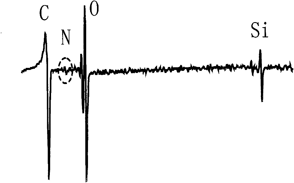
[0045] Embodiment 1 prepares nitrogen-doped graphene

[0046] 1) Defects:

[0047] ion implantation method

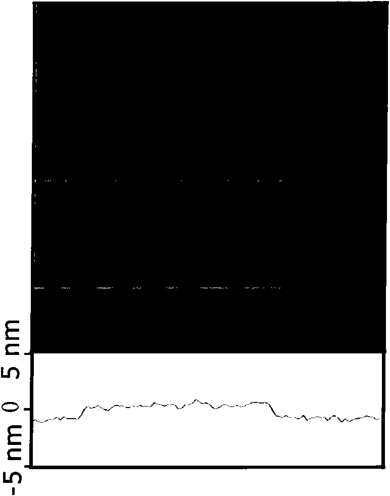
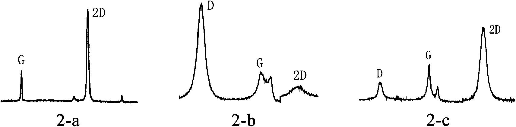
[0048] Step 1: Graphene prepared by mechanical exfoliation (flaky graphite purchased by alfa aesar), chemical vapor deposition or SiC epitaxy (references: [1] Controllable N-doping ofgraphene.DOI: 10.1021 / nl103079j; [2] ]Synthesis of N-Doped Graphene by Chemical Vapor Deposition and Its Electrical Properties. Nano Lett., Vol.9, No.5, 2009; [3] Raman spectrum of epitaxial graphene on SiC (0001), Doi: 10.1063 / 1.2929746) Enter the vacuum chamber of the ion implanter (model: LC-16, production / development unit: the 48th Research Institute of China Electronics Technology Group). Then vacuum, the vacuum degree reaches 10 -4 MPa or higher. figure 1 is the AFM image of graphene prepared by mechanical exfoliation; the Raman spectrum of graphene before ion implantation is shown as figure 2 -a shown.

[0049] Step 2: Setting parameters: Ion type: N + 、Ar + One of them or...

Embodiment 2

[0053] Embodiment 2 prepares boron doped graphene

[0054] 1) Defects:

[0055] plasma method

[0056] Step 1: Graphene prepared by mechanical exfoliation (flaky graphite purchased by alfa aesar), chemical vapor deposition or SiC epitaxy (references: [1] Controllable N-doping ofgraphene.DOI: 10.1021 / nl103079j; [2] ]Synthesis of N-Doped Graphene by Chemical Vapor Deposition and Its Electrical Properties. Nano Lett., Vol.9, No.5, 2009; [3] Raman spectrum of epitaxial graphene on SiC (0001), Doi: 10.1063 / 1.2929746) Into the vacuum chamber of the plasma machine (PS 300SA plasma system, Pfatetop, Germany) or plasma reactive etching equipment (JPCD-300, Beijing Techno Technology Co., Ltd.). Vacuum to 10 -4 MPa.

[0057] Step 2: Set parameters: one or any combination of oxygen, ammonia plasma, etc.;

[0058] Ion energy, 200eV ~ 400KeV; dose: 10 7 ~10 18 piece / cm -2

[0059] 2) Annealing:

[0060] Step 3: Put the defective graphene after plasma treatment in the annealing f...


PUM


Abstract

The invention provides a preparation method of doped graphene and a product prepared by using the method. The method comprises the following steps of: (1) processing graphene so that the graphene has defects; and (2) annealing the graphene processed in the step (1) in an atmosphere containing a doped element. The method provided by the invention can be used for controlling the electric property of graphene, is simple and reliable and is suitable for mass production. The invention also provides the application of the doped graphene prepared by using the method.

Description

technical field [0001] The invention relates to a method for preparing doped graphene. Background technique [0002] Graphene is a two-dimensional honeycomb structure with a hexagonal lattice, composed of sp 2 Single-layer atomic graphite flakes composed of hybridized carbon atoms. Research on graphene theory has been carried out for many years, but the experimental aspect has not progressed. However, since the mechanical exfoliation method of graphene prepared by Professor A.K. Geim of the University of Manchester and his collaborators in 2004, the experimental research has really begun, and it has quickly become the current research center of nanoelectronics, condensed matter physics and materials science. hotspot. The special structure of graphene makes it have many excellent properties, such as: bipolar field effect characteristics, room temperature quantum Hall effect, extremely high carrier mobility, large specific surface area, high thermal conductivity, etc. Ther...

Claims


Application Information

Patent Timeline
Patent Type & Authority Applications(China)
IPC IPC(8): H01L21/02
Inventor 宫建茹郭北斗
Owner THE NAT CENT FOR NANOSCI & TECH NCNST OF CHINA
Why Eureka
Try Eureka