Graphene preparation method based on auxiliary annealing of Ni film

A graphene and annealing technology, applied in the field of microelectronics, can solve the problems of difficulty in manufacturing graphene, expensive single crystal SiC, uneven number of layers, etc., and achieve the effects of low porosity, smooth surface and good continuity

Inactive Publication Date: 2012-06-20
XIDIAN UNIV
View PDF0 Cites 5 Cited by
  • Summary
  • Abstract
  • Description
  • Claims
  • Application Information

AI Technical Summary

Problems solved by technology

However, the single crystal SiC used in the thermal decomposition of SiC is very expensive, and the grown graphene is distributed in an island shape, the number of layers is uneven, and the size is small, so it is difficult to manufacture graphene in a large area

Method used


Image

  • Graphene preparation method based on auxiliary annealing of Ni film
  • Graphene preparation method based on auxiliary annealing of Ni film
  • Graphene preparation method based on auxiliary annealing of Ni film

Examples


Embodiment 1

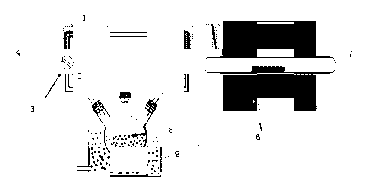
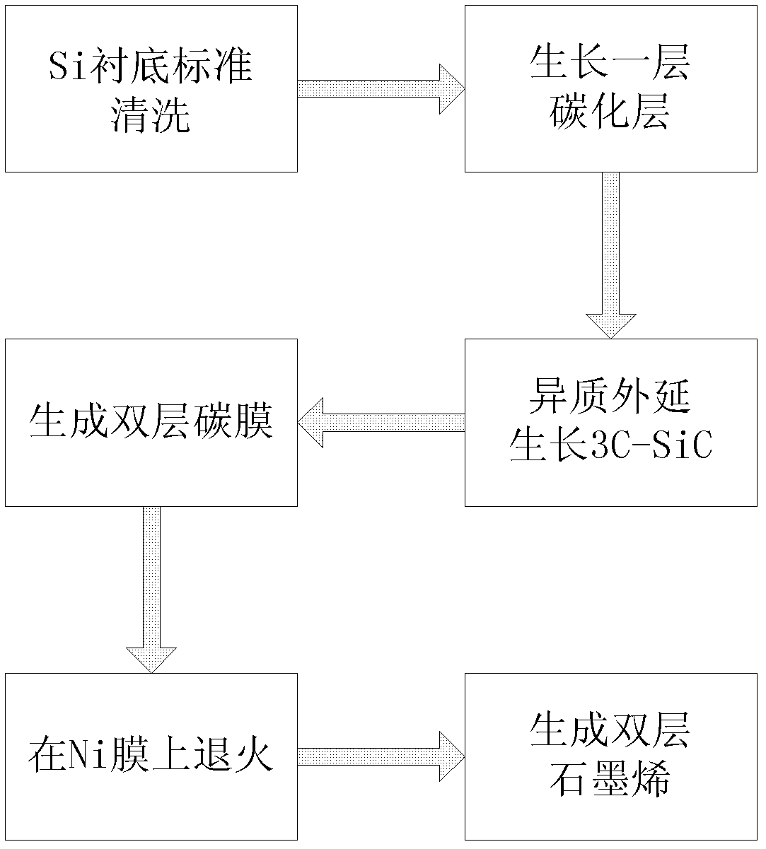
[0025] Step 1: Remove sample surface contamination.

[0026] Clean the surface of the 4-inch Si substrate substrate, that is, use NH 4 OH+H 2 o 2 Soak the sample in the reagent for 10 minutes, take it out and dry it to remove the organic residue on the surface of the sample; then use HCl+H 2 o 2 The reagent soaked the sample for 10 minutes, took it out and dried it to remove ionic contamination.

[0027] Step 2: Put the Si substrate substrate into the reaction chamber of the CVD system, and evacuate the reaction chamber to 10 -7 mbar level.

[0028] Step 3: growing the carbonized layer.

[0029] in H 2 In the case of protection, the temperature of the reaction chamber is raised to the carbonization temperature of 1000 ° C, and then the flow rate of 30ml / min is introduced into the reaction chamber. 3 h 8 , grow a layer of carbonized layer on the Si substrate, the growth time is 8min.

[0030] Step 4: growing a 3C-SiC epitaxial film on the carbonized layer.

[0031] R...

Embodiment 2

[0045] Step 1: Remove sample surface pollutants.

[0046] Clean the surface of the 8-inch Si substrate substrate, that is, use NH 4 OH+H 2 o 2 Soak the sample in the reagent for 10 minutes, take it out and dry it to remove the organic residue on the surface of the sample; then use HCl+H 2 o 2 The reagent soaked the sample for 10 minutes, took it out and dried it to remove ionic contamination.

[0047]Step 2: Put the Si substrate substrate into the reaction chamber of the CVD system, and evacuate the reaction chamber to 10 -7 mbar level.

[0048] Step 3: growing a carbonized layer.

[0049] in H 2 In the case of protection, the temperature of the reaction chamber is raised to the carbonization temperature of 1100 ° C, and then the flow rate of 30ml / min is introduced into the reaction chamber. 3 h 8 , grow a layer of carbonized layer on the Si substrate, the growth time is 6min.

[0050] Step 4: growing a 3C-SiC epitaxial film on the carbonized layer.

[0051] Rapidly...

Embodiment 3

[0060] Step A: Clean the surface of the 12-inch Si substrate, that is, use NH 4 OH+H 2 o 2 Soak the sample in the reagent for 10 minutes, take it out and dry it to remove the organic residue on the surface of the sample; then use HCl+H 2 o 2 The reagent soaked the sample for 10 minutes, took it out and dried it to remove ionic contamination.

[0061] Step B: Put the Si substrate substrate into the reaction chamber of the CVD system, and vacuumize the reaction chamber to 10 -7 mbar level.

[0062] Step C: In H 2 In the case of protection, the temperature of the reaction chamber is raised to the carbonization temperature of 1150 ° C, and then the flow rate of 30ml / min is introduced into the reaction chamber. 3 h 8 , for 3 min to grow a carbonized layer on the Si substrate.

[0063] Step D: Rapidly raise the temperature of the reaction chamber to the growth temperature of 1300°C, and feed the SiH with flow rates of 25ml / min and 50ml / min respectively. 4 and C 3 h 8 , to...


PUM


Abstract

The invention discloses a graphene preparation method based on the auxiliary annealing of a Ni film. The preparation method mainly solves the problems of small area, poor continuity and nonuniform layers of the prepared graphene in the prior art. The preparation method comprises the steps that a carburization layer is firstly grown on a 4-12-inch Si underlay substrate to be used as the transition, then, a 3C-SiC hetero epitaxy film is grown at the temperature of 1200 DEG C to 1350 DEG C, and the growth air sources are C3H8 and SiH4; then, the 3C-SiC takes reaction with gaseous CCl4 at 800 to 1000 DEG C for generating a double-layer carbon film; next, the electron beam deposition of the Ni film with the thickness being 300 to 500nm is carried out on an Si base body; the carbon surface of a generated double-layer carbon film sample sheet is placed on the Ni film, then, the sample sheet and the Ni film are simultaneously placed in Ar gas, and the annealing is carried out for 15 to 25 minutes at the temperature of 900 to 1100 DEG C for generating double-layer grapheme; and finally, the Ni film is taken away from the double-layer graphene sample sheet. The preparation method has the advantage that the double-layer grapheme has large area, smooth surface, good continuity and low porosity rate, and the double-layer grapheme can be used for sealing gas and liquid.

Description

technical field [0001] The invention belongs to the technical field of microelectronics, and relates to a semiconductor film material and a preparation method thereof, in particular to a graphene preparation method based on Ni film assisted annealing. technical background [0002] Graphene appeared in the laboratory in 2004. At that time, two scientists, Andre Gem and Kostya Novoselov, from the University of Manchester in the United Kingdom discovered that they could obtain more and more graphene in a very simple way. thinner and thinner graphite flakes. They peeled off the graphite flakes from the graphite, then glued the two sides of the flakes to a special adhesive tape, and when the tape was torn off, the graphite flakes could be split in two. Repeatedly doing this, the flakes got thinner and thinner, and eventually, they got a flake made of just one layer of carbon atoms, which is graphene. Since then, new methods of preparing graphene have emerged in an endless strea...

Claims


Application Information

Patent Timeline
Patent Type & Authority Applications(China)
IPC IPC(8): C30B25/02C30B33/02C30B29/02
Inventor 郭辉邓鹏飞张玉明张克基雷天民
Owner XIDIAN UNIV
Why Eureka
Try Eureka