A method for making resist pattern in printed circuit board production

A technology for printed circuit boards and anti-corrosion patterns, which is applied in the direction of removing conductive materials by chemical/electrolytic methods, which can solve the problems of complex production process, high cost, and impact on product accuracy, so as to improve production flexibility, improve efficiency, The effect of shortening the production process

Active Publication Date: 2015-12-02
德中(天津)技术发展股份有限公司
View PDF7 Cites 0 Cited by
  • Summary
  • Abstract
  • Description
  • Claims
  • Application Information

AI Technical Summary

Problems solved by technology

As a technological auxiliary tool to realize pattern transfer, the mask plate has a complicated manufacturing process and high cost. At the same time, it also accumulates manufacturing errors, which affects the accuracy of the final product.

Method used


Image

  • A method for making resist pattern in printed circuit board production

Examples


Embodiment Construction

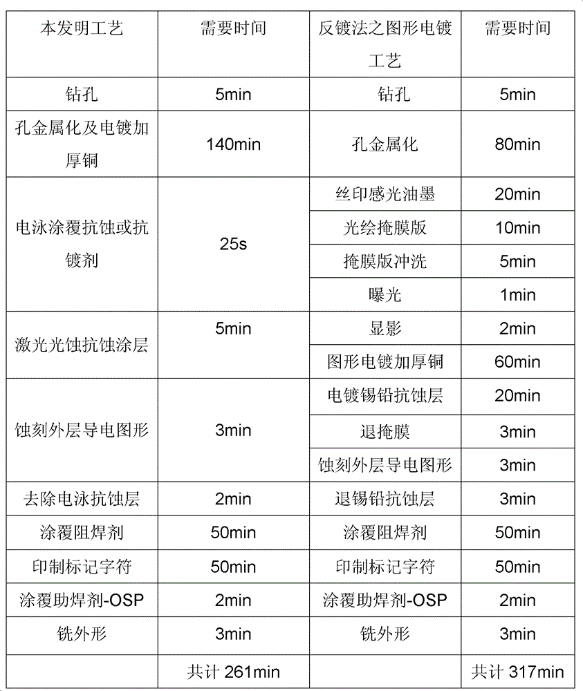
[0063] The present invention will be further described below in conjunction with an implementation example. The following implementation examples are illustrative, not restrictive, and the protection scope of the present invention cannot be limited by the following examples.

[0064] A method for manufacturing a printed circuit board using electrophoretic coating resist and laser direct formation of resist patterns, the steps of which are:

[0065] 1. Drilling: Use a DCT-M620 drilling and milling machine to drill the circuit board substrate, and the spindle speed of the drilling machine is 60000r / min. The operation steps are as follows:

[0066] (1) Place the cut copper clad laminate on the vacuum adsorption table of the drilling and milling machine, and fix it with tape around it;

[0067] (2) Import the drilling data, and configure the drilling tool according to the data requirements for the aperture;

[0068] (3) Drill holes on the copper clad laminate according to the d...


PUM


Abstract

The invention relates to a method for producing an anti-corrosion pattern in production of a printed circuit board, and the method comprises the steps of: drilling a hole, metalizing the hole, performing electrophoretic coating of a resist, producing the anti-corrosion pattern by laser, performing chemical etching and the like. The method with the electrophoretic coating of a resist and the production of the anti-corrosion pattern by the laser is adopted for replacing an existing tenting method process with the steps of hot-press lamination of an anti-corrosion photoinduced masking dry film, exposure, developing and the like or replacing the steps of pattern electroplating of an anti-corrosion metal layer and the like. According to the method disclosed by the invention, a process route for producing the anti-corrosion pattern is shortened, the operation steps are simplified, the operability is improved, the anti-corrosion coating is applied by electrophoresis, materials are easy to obtain, the operation is simple and easy, and the formed anti-corrosion coating is thin in thickness, uniform and reliable; and the anti-corrosion pattern formed by direct photoetching through the laser method is high in precision, good in an environment and great in production flexibility. The method disclosed by the invention is suitable for sample, small-batch, multi-variety and higher-precision production of the circuit boards, and is also suitable for production of ordinary circuit boards.

Description

technical field [0001] The invention is applied to the production of printed circuit boards, and is a method for making resist patterns in the production of printed circuit boards. Background technique [0002] Printed circuit board, also known as printed circuit board, printed circuit board, referred to as printed board, circuit board or circuit board, in English referred to as PCB (printed circuit board) or PWB (printed wiring board). The printed circuit board is an electronic component. According to the requirements of the design for electrical interconnection, electrical insulation and installation coordination, etc., a plane and a three-dimensional conductive pattern and insulation with holes as the main part are made on the surface and inside of the insulating material. Graphics, used to fix, install components and realize selective electrical interconnection and insulation between components. [0003] The current printed circuit board manufacturing is dominated by th...

Claims


Application Information

Patent Timeline
Patent Type & Authority Patents(China)
IPC IPC(8): H05K3/06
Inventor 沈忠存
Owner 德中(天津)技术发展股份有限公司
Why Eureka
Try Eureka