Method for designing bonding pad of surface mounted component, bonding pad structure and printing circuit board

A technology for patch components and printed circuit boards, which is applied in the direction of printed circuits, circuits, and electrical components connected by non-printed electrical components, and can solve the problems of offset or sliding, offset or sliding of patch components. , to achieve the effect of meeting the needs of heat dissipation

Active Publication Date: 2012-07-04
MAIPU COMM TECH CO LTD
View PDF4 Cites 19 Cited by
  • Summary
  • Abstract
  • Description
  • Claims
  • Application Information

AI Technical Summary

Problems solved by technology

[0006] In view of this, the embodiment of the present invention provides a pad design method for chip components to solve the problem of offset or sliding of chip components in the prior art during the reflow soldering process, and at the same time meet the heat dissipation requirements of the chip. need
[0007] The embodiment of the present invention also provides a pad design structure of chip components to solve the problem of offset or sliding of chip components in the prior art during the reflow soldering process, and at the same time meet the heat dissipation needs of the chip

Method used


Image

  • Method for designing bonding pad of surface mounted component, bonding pad structure and printing circuit board
  • Method for designing bonding pad of surface mounted component, bonding pad structure and printing circuit board
  • Method for designing bonding pad of surface mounted component, bonding pad structure and printing circuit board

Examples


Embodiment 1

[0028] see Figure 4 , is a schematic diagram of the pad design structure of the patch component pad in Embodiment 1 of the present invention; the heat dissipation pad (pad surface layer copper) 41 is 10 × 10mm, which can be divided into 9 equal parts, and the solder resist layer of the pad after equalization (solder mask) 42 is a total of 9 pieces, and the size of each piece is: 3×3mm; the pad surface steel mesh (pastmask) 43 is a total of 9 pieces, each size is: 2.8×2.8mm; between the solder mask layer of the pad There are 40 through holes 44 in total, the diameter of each through hole is 0.3 mm, and the diameter of the pad 45 of the through holes is 0.6 mm. The size of the copper on the surface of the pad meets the electrical performance requirements and completes the signal connection; at the same time, because the area of ​​the copper is large enough, it can effectively meet the heat dissipation requirements of the chip.

[0029] The solder resist layer 1 of the pad is d...

Embodiment 2

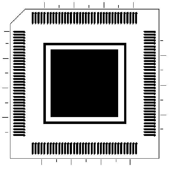
[0033] Embodiment 2 of the present invention takes a heat dissipation pad whose length×width are 18×18mm as an example, see Figure 6 , is the schematic diagram of the QFP packaging design structure after implementing the pad design method of the present invention in embodiment 2, wherein 61 is the pin welding pad around the chip component, and its pitch is 0.5mm, with 144 pins in total, and 62 is According to the size of the cooling pad of components (18×18mm), the length x width of each pad solder resist layer after equal division is 3×3mm, a total of 25 pieces, 63 for each A pad stencil corresponding to the solder mask layer of a pad, 64 is a through hole between adjacent pad solder mask layers, with a diameter of 0.5mm, and 65 is a pad with a through hole, a diameter of 0.9mm, and a total of 120 pads are used. through-hole pads. When reflow soldering, each partition of the pad of the present invention is in close contact with the cooling pin in the center of the device, a...


PUM


Abstract

The invention provides a method for designing a bonding pad of a surface mounted component. The method comprises the following steps of: modifying a design structure of a radiating bonding pad in the center of the surface mounted component, and dividing a solder mask of the bonding pad into N equal parts according to the size of the radiating bonding pad of the surface mounted component, so that the lengths or widths of the divided solder masks of the bonding pad range from 2 to 3 millimeters; and arranging a through hole array at adjacent positions of the equal parts of the divided solder masks of the bonding pad. By the method, the problem of the offset or sliding caused in the process of processing the surface mounted component by a backflow welding process is solved, and the radiating requirement of chips is met.

Description

technical field [0001] The invention relates to a technology for improving the packaging of surface mounted (Surface Mounted Technology, SMT) electronic components, in particular to a pad design method and a pad structure for preventing the sliding or offset of the SMT components. Background technique [0002] At present, the packaging technology of electronic components is developing very rapidly, and the trend of packaging is getting smaller and smaller. However, in order to solve the heat dissipation of chips, many components are packaged with special heat dissipation pads, such as Figure 1-Figure 3 The three packages shown are SOT (Small OutLine Transistor, Small Outline Transistor), QFP (Quad Flat Package, Small Square Planar Package), and QFN (Quad Flat Non-leaded package, Quad Flat Non-leaded package) package. As there are more and more pads in the package and the spacing is getting smaller and smaller, the area occupied by the heat dissipation pads is also increasing...

Claims


Application Information

Patent Timeline
Patent Type & Authority Applications(China)
IPC IPC(8): H01L21/48H01L23/488H05K1/18
Inventor 胡现辉
Owner MAIPU COMM TECH CO LTD
Why Eureka
Try Eureka