Accumulation type grooved-gate diode

A diode and accumulation type technology, applied in the field of semiconductor diode device structure, can solve the problems of easy breakdown, narrow application range, low reverse withstand voltage value, etc., and achieve the improvement of reverse recovery characteristics and forward conduction characteristics Effect

Inactive Publication Date: 2012-07-04
UNIV OF ELECTRONICS SCI & TECH OF CHINA +1
View PDF2 Cites 18 Cited by
  • Summary
  • Abstract
  • Description
  • Claims
  • Application Information

AI Technical Summary

Problems solved by technology

[0005] Since the Schottky diode has a thin reverse barrier and is prone to breakdown on its surface, the reverse breakdown voltage is relatively low, a

Method used


Image

  • Accumulation type grooved-gate diode
  • Accumulation type grooved-gate diode
  • Accumulation type grooved-gate diode

Examples


Embodiment Construction

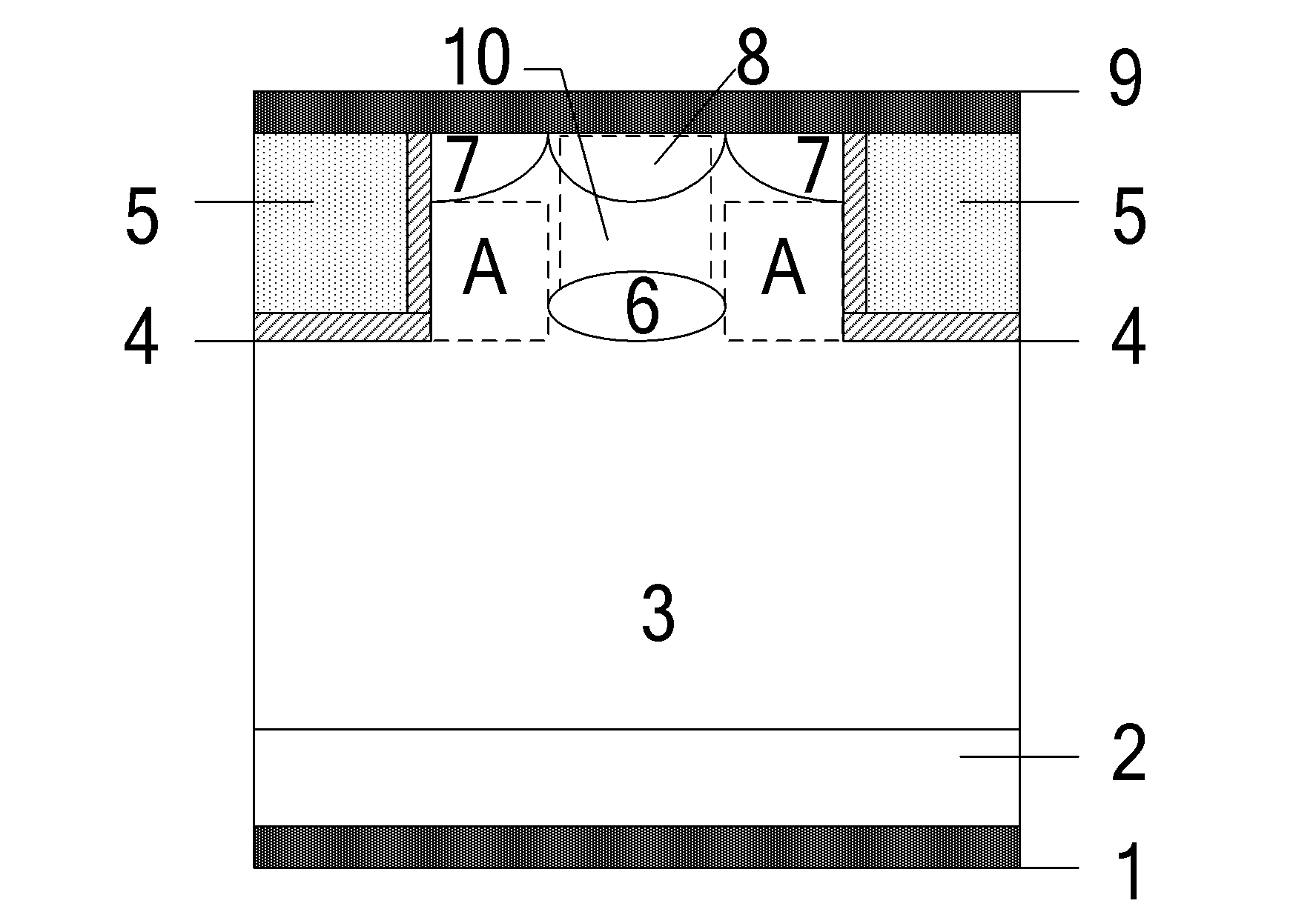
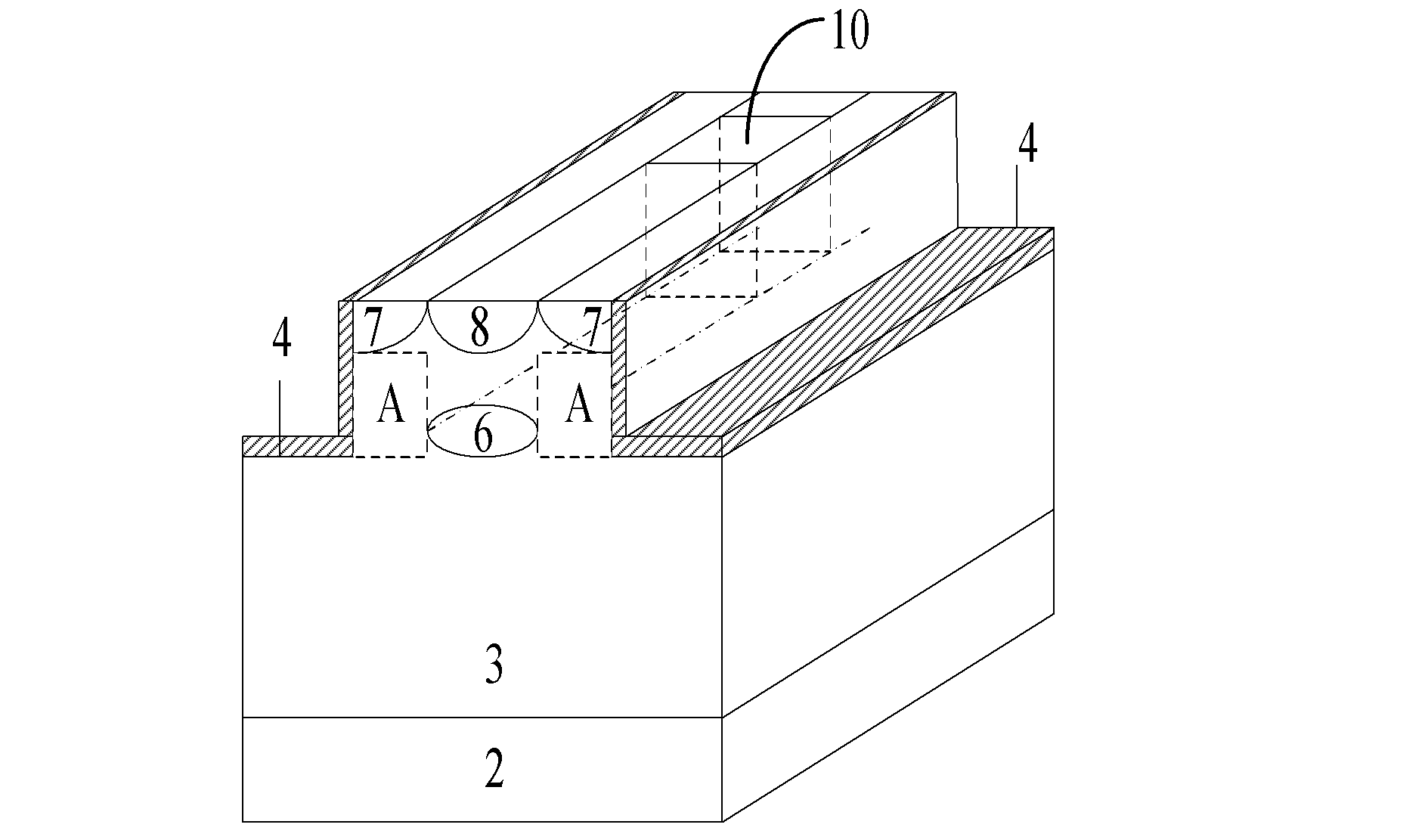
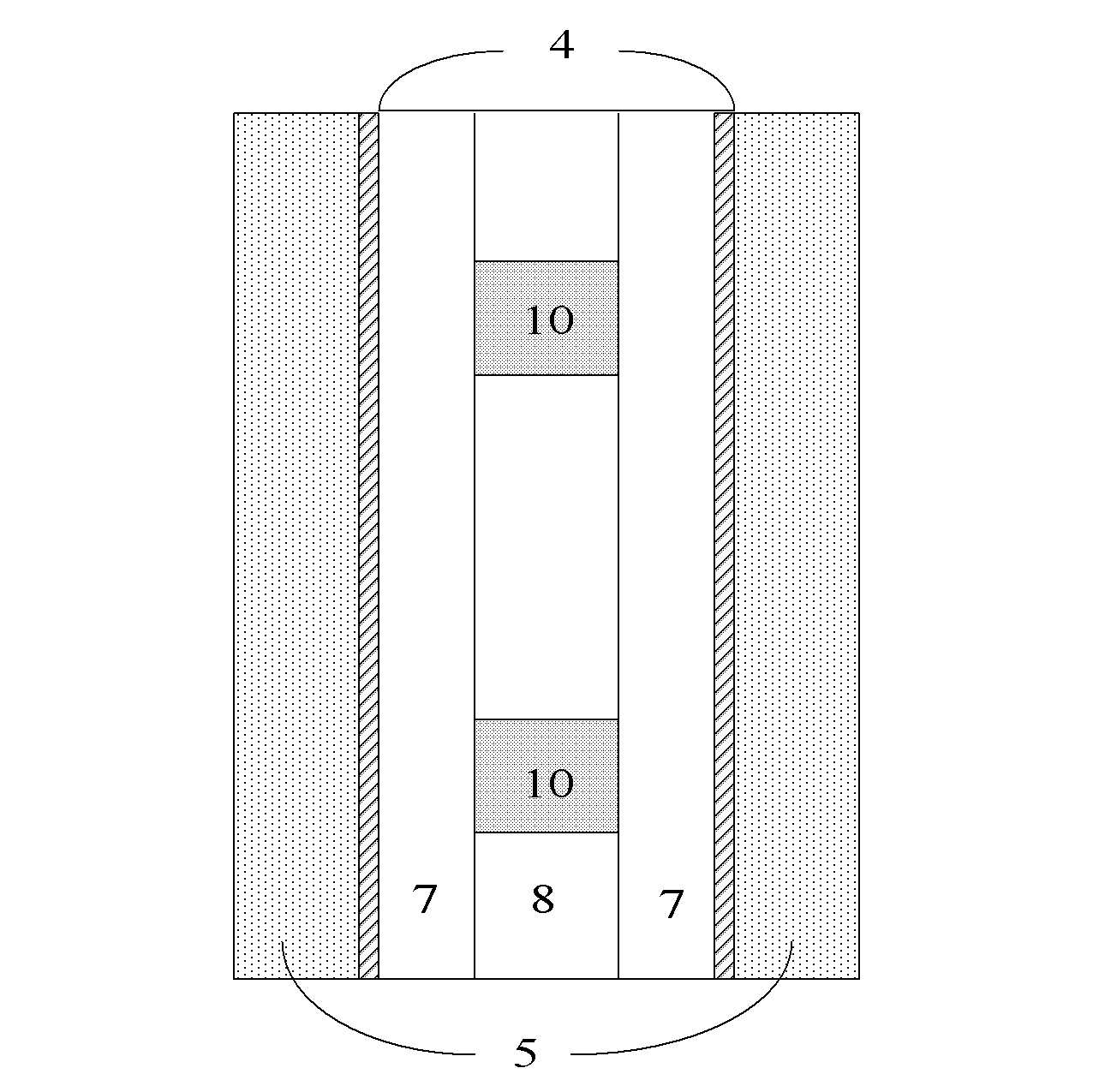
[0019] An accumulation type trench gate diode, the structure of which is as follows Figure 1~4 shown, including N + Substrate 2, located at N + The metallized cathode 1 on the back side of the substrate 2, located at N + N on the front side of substrate 2 - Drift region 3 and metallized anode 9 on top of the entire diode; in N - There is a grooved gate electrode 5 outside the two sides of the top of the drift region 3, and the two grooved gate electrodes 5 and N - The drift regions 3 are separated by respective silicon dioxide gate oxide layers 4; - There is a strip-shaped N-type heavily doped region 7 on both sides of the top of the drift region 3, and there is a strip-shaped P-type heavily doped region 8 between the two strip-shaped N-type heavily doped regions 7; N under the heavily doped region 8 and located in the middle region of the two silicon dioxide gate oxide layers 4 - There is a strip-shaped P-type buried layer region 6 in the drift region 3; there are sever...


PUM


Abstract

The invention relates to an accumulation type grooved-gate diode, belonging to the technical field of semiconductor devices. The accumulation type grooved-gate diode comprises an N<+> substrate, a metallized cathode on the back surface of the N<+> substrate and an N<-> drift region on the front surface of the N<+> substrate, wherein a slotted grid electrode and a silicon dioxide grid oxidation layer are arranged outside the two sides of the top of the N<-> drift region; two N-type heavily doped regions are respectively arranged on the two sides of the top of the N<-> drift region, and a P-type heavily doped region is arranged between the two N-type heavily doped regions; a P-type buried layer region is arranged just above the P-type heavily doped region; and a plurality of separately distributed P-type column regions are arranged between the P-type buried layer region and the P-type heavily doped region. The P-type buried layer region, the N-type heavily doped region and the silicon dioxide grid oxidation layer form a charge carrier accumulation region. According to the accumulation type grooved-gate diode disclosed by the invention, a device has smaller conduction voltage drop, shorter reverse recovery time and ultralow reverse recovery peak value current by guiding one P-type buried layer region without influencing reverse breakdown voltage and reverse leakage current.

Description

technical field [0001] The invention belongs to the technical field of semiconductor devices and relates to a semiconductor diode device structure. Background technique [0002] In electronic circuits, diodes are one of the most commonly used basic electronic components; in power electronic circuits, diodes go hand in hand with switching devices and are indispensable. Traditional rectifier diodes mainly include PN junction diodes and Schottky diodes. Among them, the PN junction diode has a large forward conduction voltage drop and a long reverse recovery time, but the PN junction diode has better stability and can work at high voltage; Schottky diode has an absolute advantage at low voltage: its forward conduction The on-voltage drop is small and the reverse recovery time is short, but the leakage current of the Schottky diode is relatively high and unstable when it reverses. In order to improve the performance of diodes, junction barrier control rectifier JBS (JBS: Juncti...

Claims


Application Information

Patent Timeline
IPC IPC(8): H01L29/861H01L29/40
Inventor 李泽宏赵起越余士江张金平任敏张波
Owner UNIV OF ELECTRONICS SCI & TECH OF CHINA
Why Eureka
Try Eureka