Circuit board and manufacturing method thereof
A circuit substrate and manufacturing method technology, applied in circuit substrate materials, printed circuit manufacturing, printed circuits, etc., can solve the problems of scrapped electronic products, low reliability of copper clad laminates, and no bonding force revealed, and achieve good bonding force, The production process is simple and the effect of mass production is easy
- Summary
- Abstract
- Description
- Claims
- Application Information
AI Technical Summary
Problems solved by technology
Method used
Image


Examples
Embodiment 1
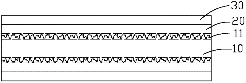
[0073] Take an aluminosilicate glass membrane with a thickness of 30 μm, wash the surface of the glass membrane with ethanol, and then put 40.2 parts by mass of hydrofluoric acid, 26.8 parts by mass of ammonium fluoride, 3.9 parts by mass of sulfuric acid, and 29.1 parts by mass of Soak in a solution composed of deionized water for 50 minutes at room temperature, take it out and rinse it with water, dry it and then treat it with a coupling agent. A rough layer with a thickness of 6 μm is formed on the upper and lower sides of the test glass film.
[0074] Put a piece on the upper and lower sides of the glass film that has formed a rough layer, and use a glass fiber cloth (1080 glass fiber cloth) with a thickness of 0.06mm to impregnate an epoxy resin adhesive (dicyandiamide curing agent) to make a FR-4 prepreg ( That is, the prepreg used for the S1141 copper clad laminate product of Guangdong Shengyi Technology) is laminated; then a copper foil is placed on the upper and lower ...
Embodiment 2
[0077] Take a piece of aluminosilicate glass film with a thickness of 100 μm that has been annealed at 500 ° C, and then put it into a film made of 22.1 parts by mass of hydrofluoric acid, 23 parts by mass of ammonium fluoride, 37.2 parts by mass of hydrochloric acid, and 17.7 parts by mass of deionized water. Soak in the formed solution for 120 minutes at room temperature, take it out and rinse it with water, dry it and then treat it with a coupling agent. A rough layer with a thickness of 15 μm is formed on the upper and lower sides of the test glass film.
[0078] Put a piece on the upper and lower sides of the glass film that has formed a rough layer, and use a glass fiber cloth (1080 glass fiber cloth) with a thickness of 0.06mm to impregnate an epoxy resin glue to make a FR-4 prepreg (that is, S1141 of Guangdong Shengyi Technology) Prepregs for copper-clad laminate products), laminated; then put a piece of copper foil on the top and bottom, and then laminated.
[0079]Pu...
Embodiment 3
[0081] Put in a container a solution consisting of 45.1 parts by mass of water glass (sodium silicate), 37.2 parts by mass of hydrochloric acid, and 17.7 parts by mass of deionized water, heat the solution to about 40°C, and stir for about 30 minutes to form a reaction solution, and then the reaction solution was slowly stirred for 24 to 48 hours to obtain an immersion plating solution. Take a piece of borosilicate glass film with a thickness of 100 μm, wash it thoroughly and put it into the immersion plating solution for 30-40 seconds to obtain a gel layer. Then lift the glass film at a uniform speed of 5-25cm / min. Then dry at 110-150° C. for 20-30 minutes. Finally, heat treatment is carried out at 400-590° C. for 30 minutes, and then naturally cooled to room temperature. Rinse with water, dry and then treat with a coupling agent. A rough layer with a thickness of 18 μm is formed on the upper and lower sides of the test glass film.
[0082] Put a piece on the upper and low...
PUM
| Property | Measurement | Unit |
|---|---|---|
| thickness | aaaaa | aaaaa |
| thickness | aaaaa | aaaaa |
| thickness | aaaaa | aaaaa |
Abstract
Description
Claims
Application Information
 - R&D
- Intellectual Property
- Life Sciences
- Materials
- Tech Scout
- Unparalleled Data Quality
- Higher Quality Content
- 60% Fewer Hallucinations
Browse by: Latest US Patents, China's latest patents, Technical Efficacy Thesaurus, Application Domain, Technology Topic, Popular Technical Reports.
© 2025 PatSnap. All rights reserved.Legal|Privacy policy|Modern Slavery Act Transparency Statement|Sitemap|About US| Contact US: help@patsnap.com