Field emission device for emitting white light
A field emission and white light technology, applied in the field of microelectronics, can solve the problems of increasing the manufacturing process of light source devices and poor stability of resin aging
- Summary
- Abstract
- Description
- Claims
- Application Information
AI Technical Summary
Problems solved by technology
Method used
Image

Examples
Embodiment 1
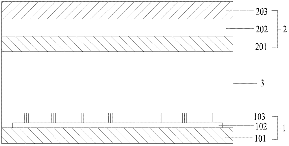
[0025] Embodiment 1, as figure 1 As shown, a device for field emission of white light includes a cathode plate assembly 1, an anode plate assembly 2 that is spaced apart from the cathode plate assembly, and a support body 3 that seals the two together, wherein the cathode plate assembly 1 includes a horizontal The cathode plate 101 is provided, the conductive cathode and grid wires 102 and the electron emission source 103 are arranged on the upper surface of the cathode plate 101 . The anode plate assembly 2 includes a transparent substrate 203, the transparent substrate 203 is cerium ion-doped YAG glass-ceramic that can absorb blue light of 420-490 nm and emit yellow light with a peak in the range of 520-590 nm, facing the cathode plate 101 The surface of the transparent substrate 203 is sequentially provided with a transparent anode 202 and a blue cathode ray luminescent material layer 201 from top to bottom. The transparent anode 202 is mainly made of indium tin oxide ITO o...
Embodiment 2
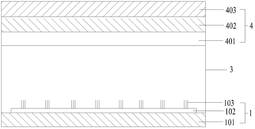
[0026] Embodiment 2, as figure 2 As shown, a device for field emission of white light includes a cathode plate assembly 1, an anode plate assembly 4 that is spaced apart from the cathode plate assembly, and a support body 3 that seals the two together. The cathode plate assembly 1 and the embodiment The structure of the cathode plate assembly in 1 is the same and will not be repeated here.
[0027] The anode plate structure 4 includes a transparent substrate 403. The transparent substrate 203 is a cerium ion-doped YAG glass-ceramic that can partially absorb 420-490nm blue light and emit yellow light with a peak in the range of 520-590nm. Directly coated with blue cathode ray luminescent material layer 402 (blue cathode ray luminescent material selects LaGaO 3 : Tm), on the blue cathodoluminescent material layer 402, a metal aluminum layer was vapor-deposited as the metal anode 401, and the coating method of the blue cathodoluminescent material layer 402 was the same as that ...
PUM
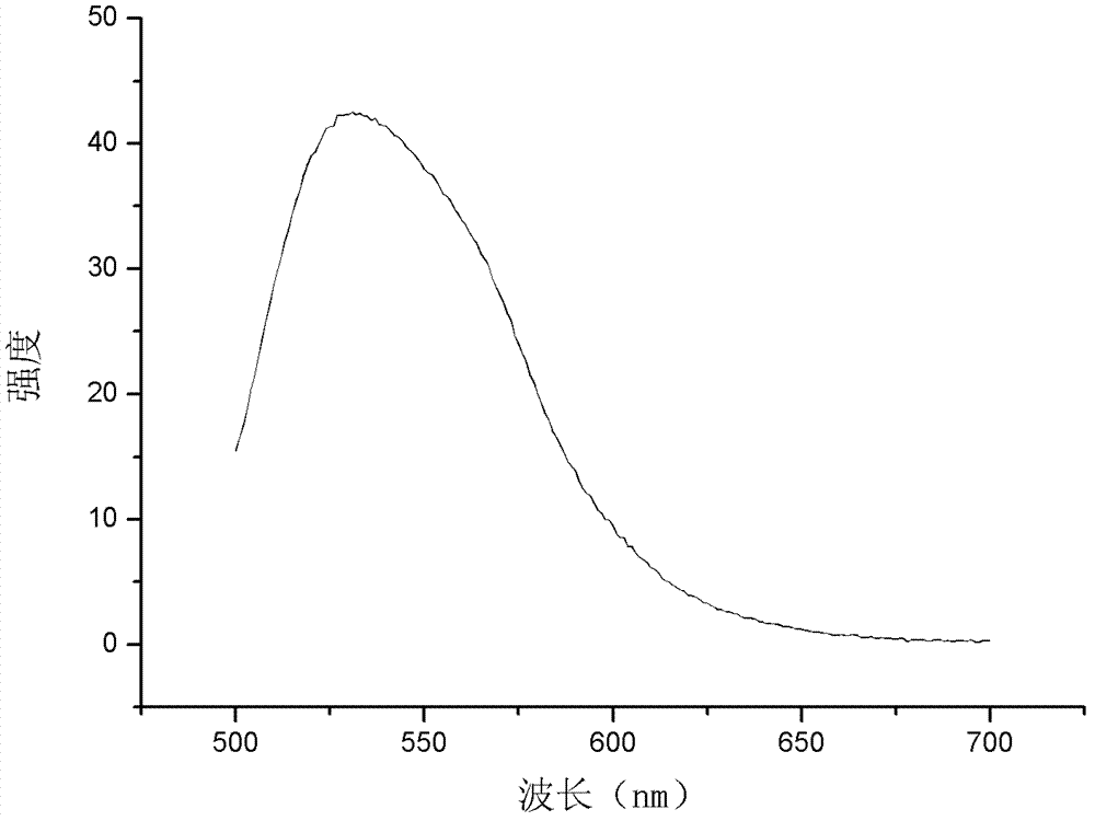
| Property | Measurement | Unit |
|---|---|---|
| wavelength | aaaaa | aaaaa |
Abstract
Description
Claims
Application Information
 - Generate Ideas
- Intellectual Property
- Life Sciences
- Materials
- Tech Scout
- Unparalleled Data Quality
- Higher Quality Content
- 60% Fewer Hallucinations
Browse by: Latest US Patents, China's latest patents, Technical Efficacy Thesaurus, Application Domain, Technology Topic, Popular Technical Reports.
© 2025 PatSnap. All rights reserved.Legal|Privacy policy|Modern Slavery Act Transparency Statement|Sitemap|About US| Contact US: help@patsnap.com