

Adjustment method of SiC (silicon carbide) single crystal flatness by wet etching
A technology of wet etching and adjustment methods, which is applied in the direction of single crystal growth, single crystal growth, chemical instruments and methods, etc., to achieve the effect of improving wafer flatness and wafer quality
- Summary
- Abstract
- Description
- Claims
- Application Information
AI Technical Summary
Problems solved by technology
Method used
Image

Examples
Embodiment 1
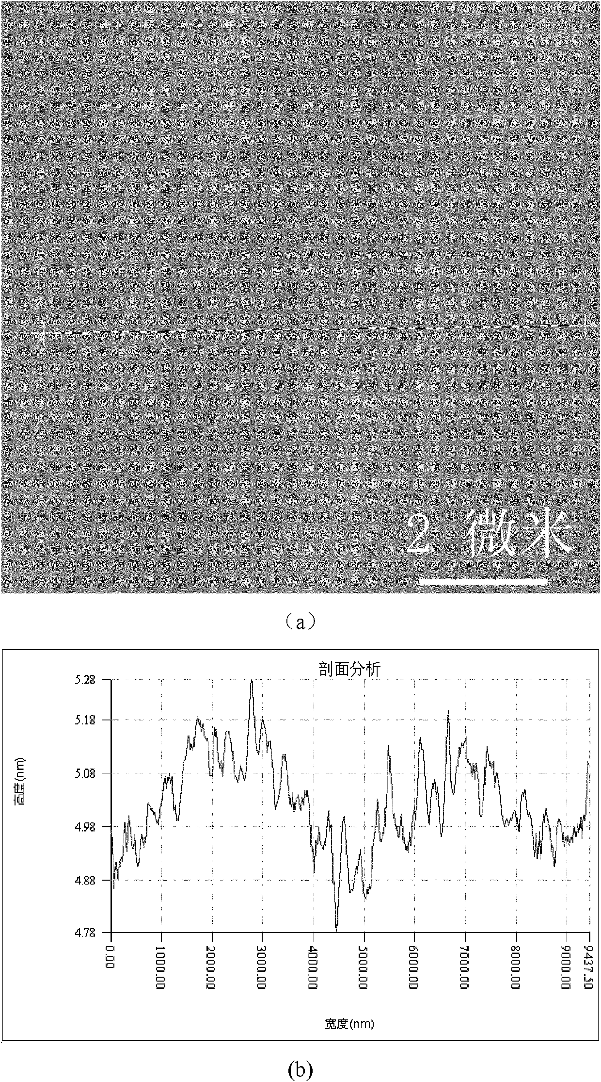
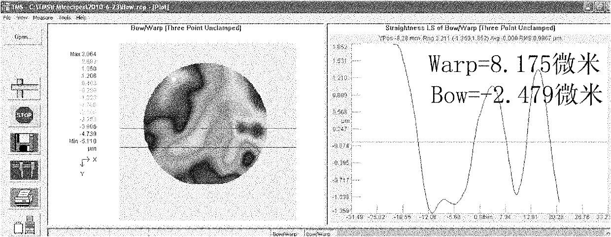
[0034] Step 1: Take a piece of silicon carbide wafer with 6H silicon surface after CMP for standard cleaning, and measure its surface TTV, Bow and Warp as: 8.996 microns, -27.520 microns, 33.456 microns respectively; its surface morphology is as follows figure 1 As shown, the RMS is 0.155 microns, and it is stored in a vacuum environment.
[0035] Step 2: Take the cleaned wafer, put it into a preheating furnace and preheat it to 350° C. for 10 minutes, and set it aside.
[0036]Step 3: Add 1 kg of KOH+NaOH mixture into an aluminum oxide crucible in a ratio of 1:1, raise the temperature to 310°C, wait for half an hour, and then add 100 grams of potassium carbonate as an additive until the entire crucible is melted. Clear, let stand for 20 minutes, blow into oxygen, the flow rate of oxygen blowing is controlled at 200 standard milliliters per minute.
[0037] Step 4: Take the preheated wafer, put it in the molten molten pool, blow oxygen for 10 seconds, take out the samples ran...
Embodiment 2
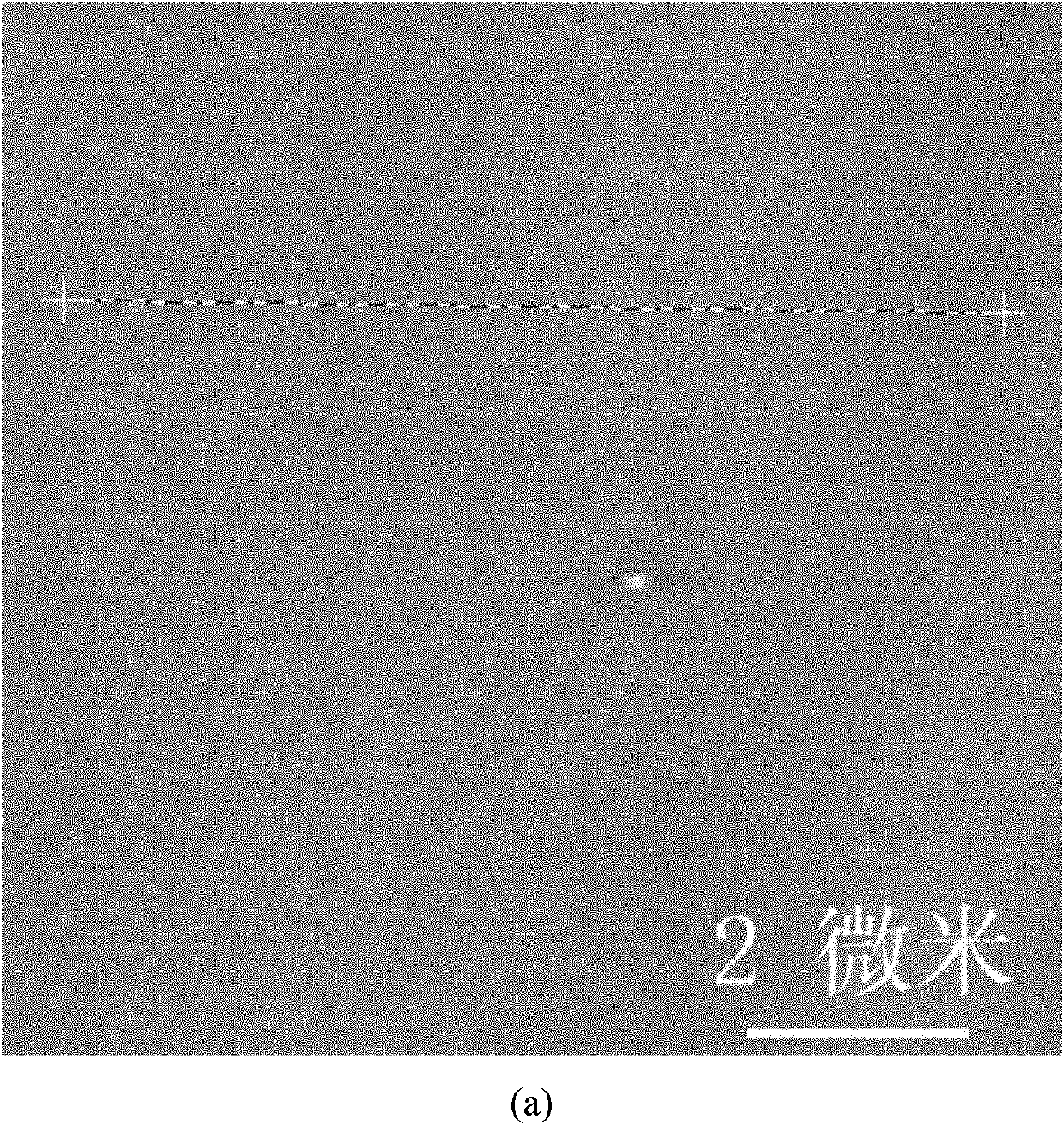
[0042] Step 1: Take a vanadium-doped semi-insulating 2-inch 4H-SiC (0001) silicon surface polished wafer after CMP for standard cleaning, and measure its surface TTV, Bow and Warp as: 9.332 microns, -22.777 microns, 28.490 microns ; its surface morphology is as Figure 4 As shown, the RMS is 0.130 microns, and it is stored in a vacuum environment.
[0043] Step 2: Take the cleaned wafer, put it into a preheating furnace and preheat it to 500° C. for 10 minutes, and set it aside.
[0044] Step 3: Add 1 kg of KOH+NaOH mixture into an aluminum oxide crucible at a ratio of 2:1, heat up to 350°C, wait for 40 minutes, and then add 70 grams of potassium carbonate as an additive until the entire crucible is melted. Clear, let stand for 20 minutes, blow into oxygen, the flow of oxygen blowing is controlled at 300 standard milliliters per minute.
[0045] Step 4: Take the preheated wafer, put it in the molten molten pool, blow oxygen for 15 seconds, take out the samples randomly, and ...
Embodiment 3
[0050] Step 1: Take a 3-inch nitrogen-doped 6H-SiC (0001) silicon surface polished wafer after CMP for standard cleaning, and measure its surface TTV, Bow and Warp as: 13.012 microns, -44.259 microns, 61.925 microns; Surface morphology such as Figure 7 As shown, the RMS is 0.223 microns, and it is stored in a vacuum environment.
[0051] Step 2: Take the cleaned wafer, put it into a preheating furnace and preheat it to 500° C. for 10 minutes, and set it aside.
[0052] Step 3: Add 2 kg of KOH+NaOH mixture into an aluminum oxide crucible at a ratio of 3:1, heat up to 400°C, wait for 60 minutes, and then add 300 grams of potassium carbonate as an additive until the entire crucible is melted. Clear, let stand for 30 minutes, blow into oxygen, the flow of oxygen blowing is controlled at 300 standard milliliters per minute.
[0053] Step 4: Take the preheated wafer, put it in the molten molten pool, blow oxygen for 20 seconds, take out the samples randomly, and dry them on the s...
PUM
 Abstract
Description
Claims
Application Information