Method for realizing high-performance copper interconnection by using upper mask

A high-performance, copper interconnection technology, applied in electrical components, semiconductor/solid-state device manufacturing, circuits, etc., can solve the problems of unfavorable etching process etching shape and size, reduce interconnection reliability, and difficult to fill completely , to achieve the effect of reducing chip interconnection resistance, increasing process difficulty, and reducing interconnection resistance

Inactive Publication Date: 2012-07-11
SHANGHAI HUALI MICROELECTRONICS CORP
View PDF5 Cites 2 Cited by
  • Summary
  • Abstract
  • Description
  • Claims
  • Application Information

AI Technical Summary

Problems solved by technology

Because the thickness is too thick, it means that the depth of the trench structure is very large, which will not be conducive to the etching process to control the shape and size of the etching, and the metal filling process is also difficult to complete the complete filling, which will increase the resistance and reduce the interconnection. reliability, with a very detrimental effect on

Method used


Image

  • Method for realizing high-performance copper interconnection by using upper mask
  • Method for realizing high-performance copper interconnection by using upper mask
  • Method for realizing high-performance copper interconnection by using upper mask

Examples


Embodiment Construction

[0045] The present invention will be further described below in conjunction with the accompanying drawings and specific embodiments, but not as a limitation of the present invention.

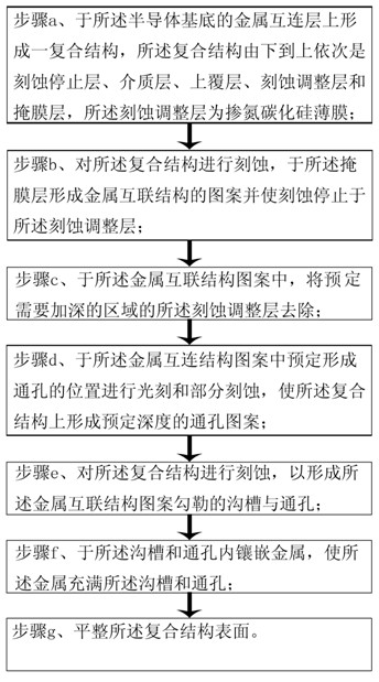
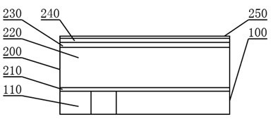
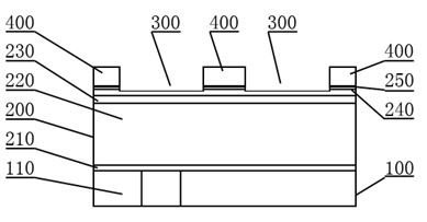
[0046] Such as figure 1 As shown, a method for realizing high-performance copper interconnection by using an upper mask in the present invention includes a semiconductor substrate 100 with a metal interconnection layer 110, and includes the following specific steps:

[0047] Such as figure 2 As shown, in step a, a composite structure 200 is formed on the metal interconnection layer 110 of the semiconductor substrate 100. The composite structure 200 consists of an etch stop layer 210, a dielectric layer 220, an upper cladding layer 230, and an etch adjustment layer from bottom to top. layer 240 and mask layer 250.

[0048] Wherein the etching stop layer 210 is a nitrogen-doped silicon carbide layer, and its formation method can be chemical vapor deposition; the dielectric layer 220 can be flu...


PUM

PropertyMeasurementUnit
thicknessaaaaaaaaaa
relative permittivityaaaaaaaaaa

Abstract

The invention discloses a method for realizing high-performance copper interconnection by using an upper mask. The upper mask comprises a semiconductor substrate in a metal interconnecting layer, wherein a composite structure is formed on the metal interconnecting layer of the semiconductor substrate; the composite structure consists of an etching stop layer, a medium layer, an upper coating layer, an etching adjusting layer and a mask layer from bottom to top; and the etching adjusting layer is a nitrogen-doped silicon carbide thin film. The method has the advantages that: according to the technical flow and the method provided by the invention, the depth of a copper interconnecting line ditch is selectively changed by using the added nitrogen-doped silicon carbide to etch a depth-adjusting layer, so the square resistance of a copper interconnecting line which is in accordance with a condition in a specific area is reduced, and the aim of selectively reducing chip interconnecting resistance is fulfilled. According to the application of the method, the interconnecting resistance can be reduced to the great extent on the premise that the overall copper interconnection depth is not changed, the process difficulty is not increased, and the size of a technical window is not reduced, the signal delay of a chip is reduced, the loss is reduced, and the overall performance of a chip is improved.

Description

technical field [0001] The invention relates to the field of semiconductor manufacturing, in particular to a method for realizing high-performance copper interconnection by using an upper mask. Background technique [0002] In the semiconductor integrated circuit industry, high-performance integrated circuit chips require high-performance back-end electrical connections. Due to its low resistivity properties, metallic copper has been more and more widely used in advanced integrated circuit chips. From aluminum wires to copper wires, the material change brought about a huge reduction in resistivity. With the advancement of integrated circuit technology, the complexity of the chip increases, which means that the resistance of the back-end interconnection lines in the chip becomes one of the bottlenecks of performance. How to effectively reduce the resistance has become an important research topic for back-end interconnection. [0003] From the resistance formula, we can get...

Claims


Application Information

Patent Timeline
Patent Type & Authority Applications(China)
IPC IPC(8): H01L21/768
Inventor 张亮李磊胡友存姬峰陈玉文
Owner SHANGHAI HUALI MICROELECTRONICS CORP
Why Eureka
Try Eureka