

Double-layer isolation longitudinal stacked semiconductor nanowire MOSFET (Metal Oxide Semiconductor Field Effect Transistor)
A vertical stacking, semiconductor technology, applied in the direction of semiconductor devices, electrical components, circuits, etc., can solve the problems of difficult process, limited device current driving capability, inability to adjust the gate work function, etc., to achieve high device integration, improve electrical performance, the effect of increasing the current drive capability of the device
- Summary
- Abstract
- Description
- Claims
- Application Information
AI Technical Summary
Problems solved by technology
Method used
Image

Examples
Embodiment Construction
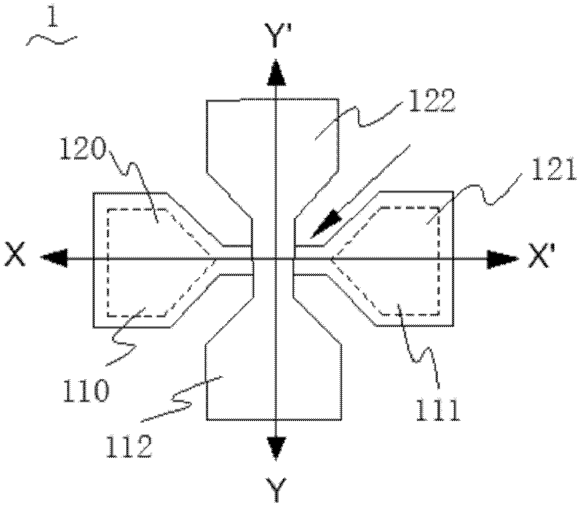
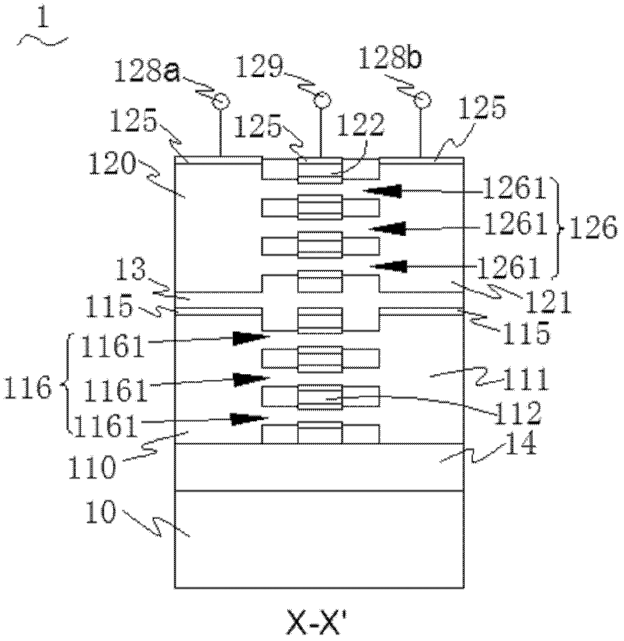
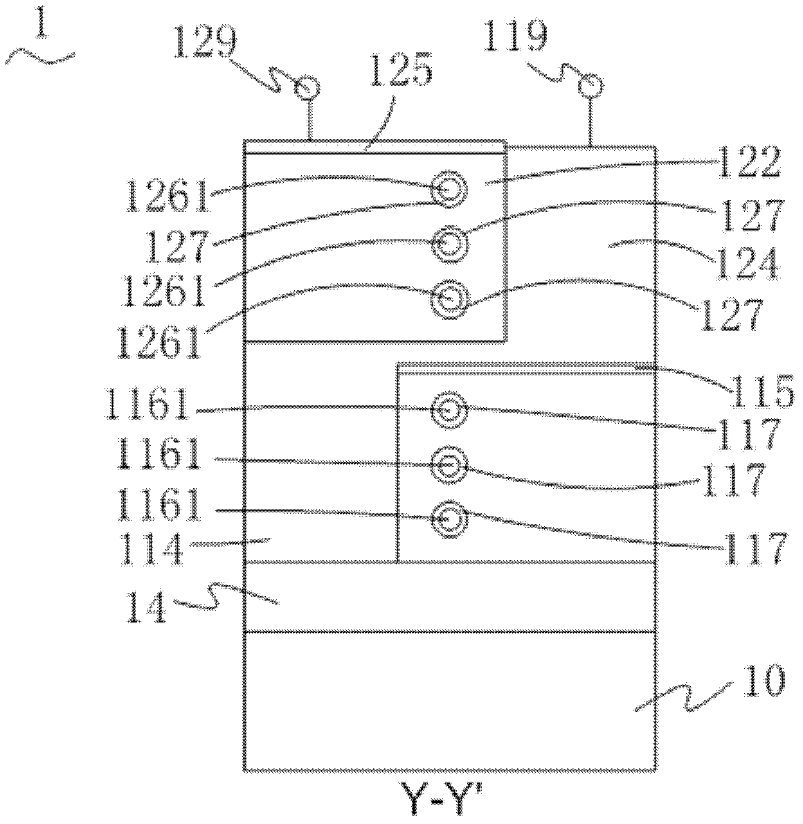
[0047] In order to illustrate the technical content, structural features, achieved goals and effects of the present invention in detail, the following will be described in detail in conjunction with the embodiments and accompanying drawings. Wherein, the first semiconductor nanowire group may include a plurality of first semiconductor nanowires arranged in a vertical stack, three are taken as an example in the embodiments and drawings, and the second semiconductor nanowire group may include a plurality of For the second semiconductor nanowires arranged in a vertical stack, three are used as an example in the embodiments and drawings.
[0048] Please refer to FIG. 1(a), FIG. 1(b), and FIG. 1(c). FIG. 1(a) shows a schematic top view of the double-layer isolation vertically stacked semiconductor nanowire MOSFET of the present invention. Figure 1(b) is a schematic cross-sectional view of Figure 1(a) along the X-X' direction. Figure 1(c) is a schematic cross-sectional structure di...
PUM
 Abstract
Description
Claims
Application Information