Semiconductor device and process for production thereof
A manufacturing method, semiconductor technology, applied in semiconductor/solid-state device manufacturing, semiconductor devices, semiconductor/solid-state device components, etc., to achieve the effects of increasing switching speed, reducing injection times, and low on-resistance
- Summary
- Abstract
- Description
- Claims
- Application Information
AI Technical Summary
Problems solved by technology
Method used
Image

Examples
no. 1 Embodiment approach
[0091] Hereinafter, a first embodiment of the present invention will be described with reference to the drawings. In the following drawings, components having substantially the same functions as components of conventional semiconductor devices are assigned the same reference numerals. The present invention is not limited to the following embodiments. In addition, the first conductivity type may be either n-type or p-type, and in this case, the second conductivity type is p-type or n-type.
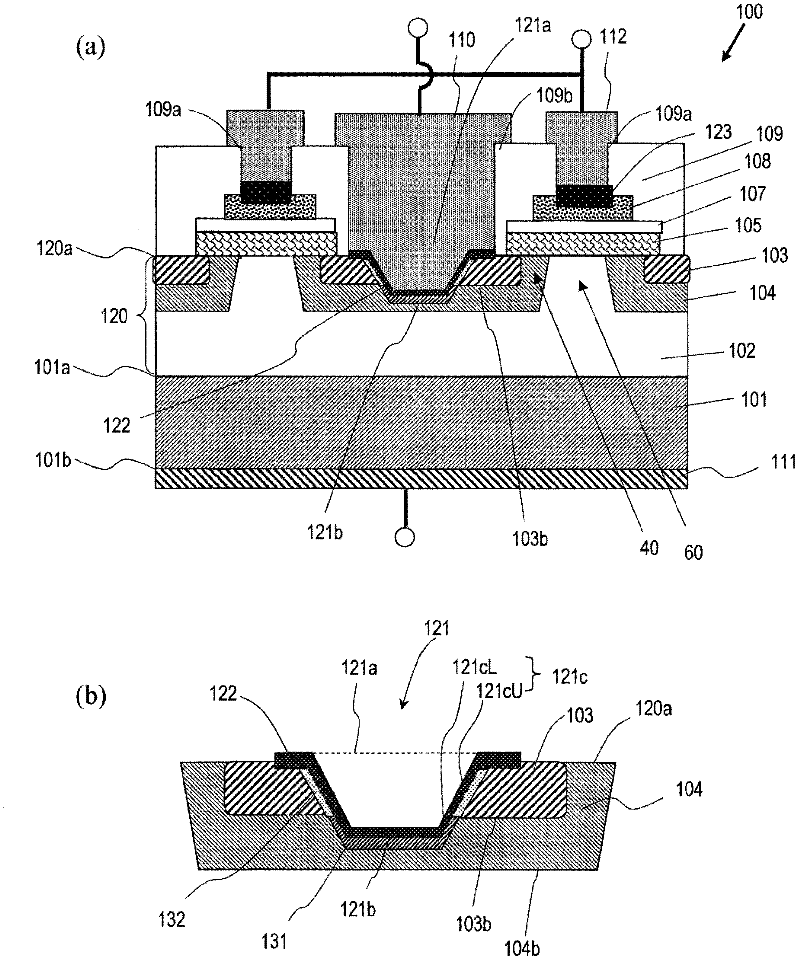
[0092] figure 1 (a) schematically shows the cross-sectional structure of the semiconductor device 100 according to the first embodiment of the present invention. The semiconductor device 100 includes a first conductivity type semiconductor substrate 101 having a main surface 101 a and a back surface 101 b and containing silicon carbide. A first silicon carbide layer of the first conductivity type is provided on the main surface 101 a of the semiconductor substrate 101 . The first silic...
no. 2 Embodiment approach
[0145] Hereinafter, a second embodiment of the present invention will be described with reference to the drawings.
[0146] Figure 14 (a) is a schematic cross-sectional view of a semiconductor device 200 according to a second embodiment of the present invention, Figure 14 (b) is an enlarged cross-sectional view showing a contact trench structure in the semiconductor device 200 .
[0147] In the semiconductor device 200 , the sidewall lower portion 121cL of the contact trench 121 is inclined more than the sidewall upper portion 121cU. In addition, the second impurity region 132 ( figure 1 ). The first ohmic electrode 122 is in contact with the first impurity region 103 at the upper surface 120 a of the first silicon carbide layer 120 and the upper sidewall 121 cU of the contact trench 121 . Other composition and figure 1 The configuration shown is the same.
[0148] According to the present embodiment, the contact area between the contact region 131 and the first ohmi...
no. 3 Embodiment approach
[0160] Hereinafter, a third embodiment of the semiconductor device of the present invention will be described with reference to the drawings. Here, although a vertical silicon carbide MISFET is described as an example, the semiconductor device of the present invention is not limited to the illustrated example as long as it includes a silicon carbide layer and an ohmic electrode forming an ohmic contact with the silicon carbide layer. .
[0161] In the following drawings, there is a comparison with existing semiconductor devices ( Figure 37 ) components that have substantially the same function are given the same reference signs. In addition, the first conductivity type may be either n-type or p-type, and the second conductivity type is a conductivity type (p-type or n-type) different from the first conductivity type.
[0162] Figure 17 (a) schematically shows the cross-sectional structure of the semiconductor device 300 of the present embodiment. The semiconductor device ...
PUM
 Abstract
Description
Claims
Application Information
 - R&D
- Intellectual Property
- Life Sciences
- Materials
- Tech Scout
- Unparalleled Data Quality
- Higher Quality Content
- 60% Fewer Hallucinations
Browse by: Latest US Patents, China's latest patents, Technical Efficacy Thesaurus, Application Domain, Technology Topic, Popular Technical Reports.
© 2025 PatSnap. All rights reserved.Legal|Privacy policy|Modern Slavery Act Transparency Statement|Sitemap|About US| Contact US: help@patsnap.com