Integrated optical chip based on glass-based ion exchange buried optical waveguide and manufacturing method

An ion exchange, integrated optics technology, applied in the directions of light guide, optics, optical components, etc., can solve the problems of high process requirements, large polarization dependence, affecting the stability and reliability of the chip, and achieve short process steps, low cost, low stress effect

Inactive Publication Date: 2012-07-18
上海光芯集成光学股份有限公司
View PDF4 Cites 12 Cited by
  • Summary
  • Abstract
  • Description
  • Claims
  • Application Information

AI Technical Summary

Problems solved by technology

Although the integrated optical chip based on PECVD technology has good optical characteristics, it has a large polarization dependence due to the rectangular cross-section of the waveguide region, and the manufacturing method of the integrated

Method used


Image

  • Integrated optical chip based on glass-based ion exchange buried optical waveguide and manufacturing method
  • Integrated optical chip based on glass-based ion exchange buried optical waveguide and manufacturing method
  • Integrated optical chip based on glass-based ion exchange buried optical waveguide and manufacturing method

Examples


Embodiment 1

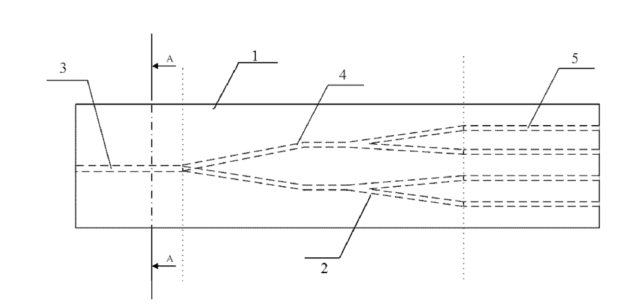
[0043] Such as Figure 1-4 As shown, a 1×4 optical splitter chip based on a glass-based ion-exchange buried optical waveguide is used for illustration.

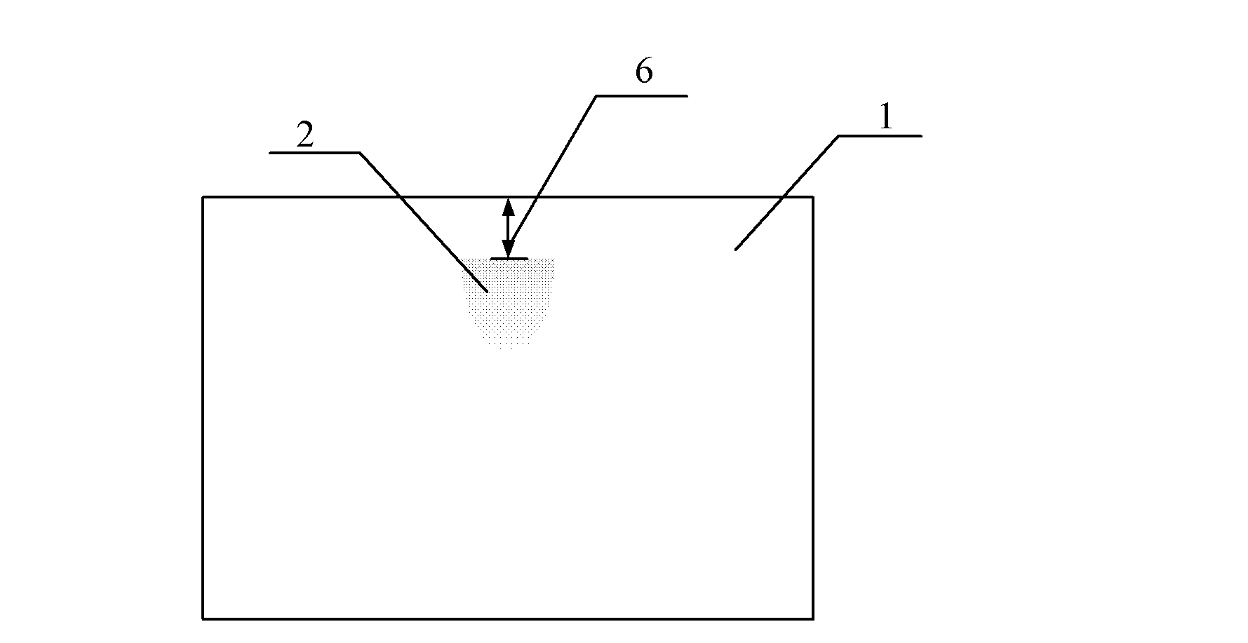
[0044] The chip is mainly composed of a glass substrate 1 and an ion exchange buried optical waveguide 2; the ion exchange buried optical waveguide 2 is located inside the glass substrate 1, and the distance 6 from the upper surface of the glass substrate is 15 μm. The ion exchange buried optical waveguide is divided into three parts in the horizontal direction in the glass substrate: the input waveguide area 3, the functional structure area 4 and the output waveguide area 5, and the functional structure area 4 is connected to the input waveguide area 3 and the output waveguide area 5 , in this embodiment, the input waveguide area 3 is an input single-port straight waveguide area, the functional structure area 4 is a cascaded branch structure area, and the output waveguide area 5 is an output four-port straight waveguide arra...

Embodiment 2

[0047] see Figure 1-4 As shown, a 2×2 optical coupler chip based on a glass-based ion-exchange buried optical waveguide is mainly composed of a glass substrate and an ion-exchange buried optical waveguide; the ion-exchange buried optical waveguide is located inside the glass substrate. The distance 6 from the upper surface of the glass substrate is 7000 μm. The ion exchange buried optical waveguide is divided into three parts in the glass substrate: the input two-port straight waveguide array area, the 2×2 coupling area and the output two-port straight waveguide array area. The integral ion-exchange buried optical waveguide realizes the function of 2×2 optical coupler. The ion-exchange buried optical waveguide is a graded-refractive-index waveguide. The vertical cross-sectional profile is in the shape of a "comet". The refractive index near the "comet nucleus" is the largest, and the refractive index of the outward part gradually decreases, showing a "comet tail" distributio...

Embodiment 3

[0050] An integrated optical chip based on a glass-based ion exchange buried optical waveguide, the integrated optical chip is mainly composed of a glass substrate and an ion exchange buried optical waveguide; the upper side of the waveguide of the ion exchange buried optical waveguide is not completely separated from the upper surface of the glass substrate , the distance between the ion-exchange buried optical waveguide and the upper surface of the glass substrate is 0 μm.

[0051] The ion-exchange buried optical waveguide is a graded-index waveguide, which is divided into three regions in the horizontal direction in the glass substrate: the input waveguide region, the functional structure region and the output waveguide region, and the functional structure region is connected to the input waveguide area and the output waveguide area. Wherein: the input waveguide area is composed of a single straight waveguide; the structure of the functional structural area is a shunt struc...


PUM

PropertyMeasurementUnit
Thicknessaaaaaaaaaa
Thicknessaaaaaaaaaa
Thicknessaaaaaaaaaa

Abstract

The invention relates to an integrated optical chip based on a glass-based ion exchange buried optical waveguide and a manufacturing method. The integrated optical chip mainly comprises a glass substrate and an ion exchange buried optical waveguide; and the ion exchange buried optical waveguide is positioned in the glass substrate, and the distance between the ion exchange buried optical waveguide and the upper surface of the glass substrate is 0 to 7,500 microns. The manufacturing method comprises the following steps of: coating, photoetching, corrosion, glue removal, primary exchange, secondary exchange, scribing, grinding and polishing. Compared with the prior art, the invention has the advantages that polarization dependency of the chip can be reduced, the internal stress of the chip can be eliminated, and the chip has long service life, stability, reliability and the like.

Description

technical field [0001] The invention relates to an integrated optical chip in the field of optical communication, in particular to an integrated optical chip based on a glass-based ion exchange buried optical waveguide and a manufacturing method. Background technique [0002] At present, integrated optical chips used in optical communication on the market are mainly manufactured based on PECVD technology. PECVD technology is a plasma-enhanced chemical vapor deposition technology. Its technical principle is: use low-temperature plasma as an energy source, place the wafer on the cathode of glow discharge under low pressure, and use glow discharge or an additional heating element to heat up the sample. To the predetermined temperature, and then pass in an appropriate amount of reaction gas, the gas is ionized under the action of microwave or radio frequency, and plasma is formed locally. Because the plasma is very active, the gas reacts with the plasma through a series of chemi...

Claims


Application Information

Patent Timeline
IPC IPC(8): G02B6/122G02B6/125G02B6/138
Inventor 郑伟伟王毅强王明华杨建义郝寅雷商惠琴
Owner 上海光芯集成光学股份有限公司
Why Eureka
Try Eureka