Method by adopting impulse airflow method to grow gallium phosphide (GaP) current extension layer

A technology of current spreading layer and pulsed air flow, applied in crystal growth, single crystal growth, single crystal growth and other directions, can solve the problems of affecting the efficiency and life of LED, reducing light extraction efficiency and so on

Active Publication Date: 2012-07-18
XIAMEN CHANGELIGHT CO LTD
View PDF4 Cites 13 Cited by
  • Summary
  • Abstract
  • Description
  • Claims
  • Application Information

AI Technical Summary

Problems solved by technology

The second electrode 7 is generally composed of an opaque metal alloy, so most of the light emitted by the effective light-emitting area 8 is shielded by the second electrode 7, which reduces t

Method used


Image

  • Method by adopting impulse airflow method to grow gallium phosphide (GaP) current extension layer
  • Method by adopting impulse airflow method to grow gallium phosphide (GaP) current extension layer
  • Method by adopting impulse airflow method to grow gallium phosphide (GaP) current extension layer

Examples


Embodiment Construction

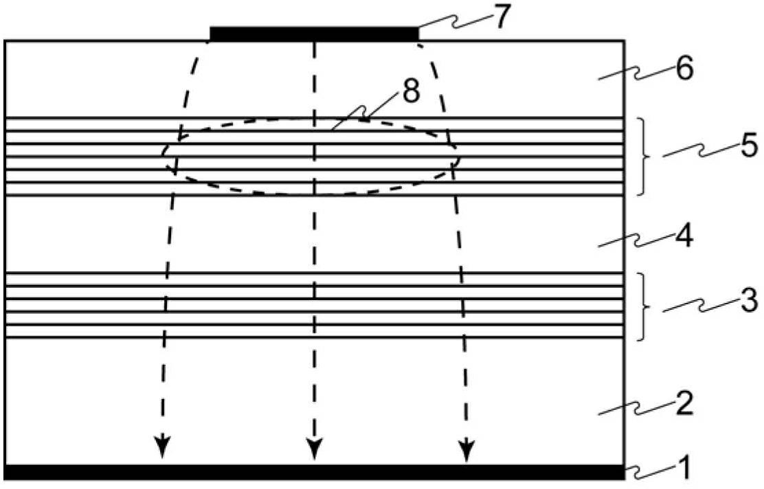
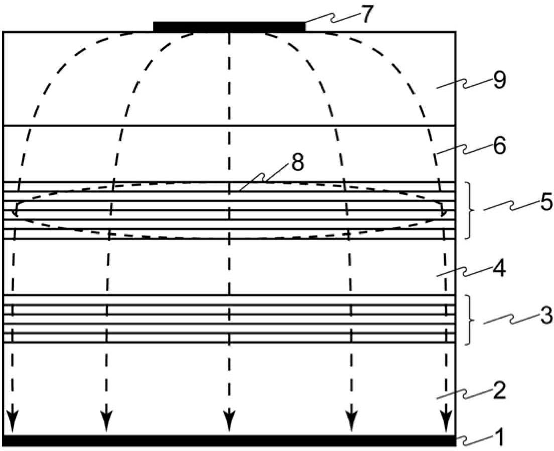
[0020] Such as figure 2 As shown, a distributed Bragg reflection layer 3 , a first-type epitaxial layer 4 , a light-emitting layer 5 and a second-type epitaxial layer 6 are sequentially grown on a GaAs substrate 2 by MOCVD. The distributed Bragg reflection layer 3 is composed of a combination of AlAs, GaAs, AlGaAs, AlInP, GaInP, and AlGaInP. The first-type epitaxial layer 4 is composed of AlAs, GaAs, AlGaAs, AlInP, GaInP, AlGaInP, and is doped with first-type impurities. The light emitting layer 5 is composed of AlAs, GaAs, AlGaAs, AlInP, GaInP, AlGaInP. The second-type epitaxial layer 6 is composed of AlAs, GaAs, AlGaAs, AlInP, GaInP, AlGaInP, and is doped with second-type impurities.

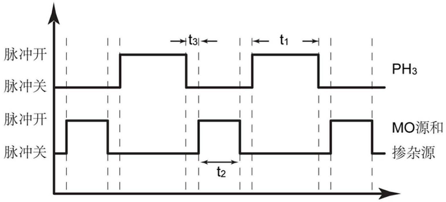
[0021] On the second-type epitaxial layer 6, the metal-organic compound source (MO source) containing gallium atoms, phosphine (PH 3 ) and the dopant source are pulsed into the MOCVD reaction chamber. The GaP current spreading layer 9 is grown by using the first pulse working mode or the ...


PUM


Abstract

The invention discloses a method by adopting an impulse airflow method to grow a gallium phosphide (GaP) current extension layer, which is characterized in that: a molybdenum (MO) source containing gallium atoms, phosphorane and a doping source are alternatively introduced into a reaction chamber of a metal organic chemical gas-phase precipitation system in a pulse way, or the flow-rate of the phosphorane is maintained constant, the MO source containing t he gallium atoms and the doping source are introduced in a pulse way. Due to adoption of the method, transition time of gallium atoms and phosphorus atoms on the surface of an extension layer can be increased, so that the gallium atoms and the phosphorus atoms can adequately cover the surface of the extension layer, and a GaP current extension layer with high quality can be obtained.

Description

technical field [0001] The invention relates to a method for growing a high-quality GaP current spreading layer in an AlGaInP-based light-emitting diode (LED), by pulse-feeding an MO source containing gallium atoms, phosphine (PH 3 ) and doping sources to increase the migration time of atoms on the surface of the epitaxial layer, so that it can fully cover the surface of the epitaxial layer, thereby obtaining a high-quality GaP current spreading layer. Background technique [0002] Semiconductor light-emitting diodes (LEDs) have attracted more and more attention due to their high efficiency, energy-saving and environmental protection characteristics, and have gradually been applied to daily life, such as traffic lights, outdoor display screens, night scene lighting, backlights for mobile phones and LCD TVs source etc. The structure of an AlGaInP LED without a current spreading layer is as figure 1 As shown, it is mainly composed of a first electrode 1 , a substrate 2 , a d...

Claims


Application Information

Patent Timeline
IPC IPC(8): H01L33/00C30B25/02C30B29/44
Inventor 陈凯轩张银桥蔡建九张永林志伟单智发张双翔占荣王向武
Owner XIAMEN CHANGELIGHT CO LTD
Why Eureka
Try Eureka