Wafer suitable for nanometer technology and method for manufacturing the same

A manufacturing method and wafer technology, applied in semiconductor/solid-state device manufacturing, electrical components, circuits, etc., can solve problems such as inconvenience, general products and methods do not have appropriate structures and methods, and achieve low manufacturing costs and quality uniformity. The effect of improving the utilization rate of crystal pillars

Inactive Publication Date: 2012-08-01
陈柏颖
View PDF5 Cites 4 Cited by
  • Summary
  • Abstract
  • Description
  • Claims
  • Application Information

AI Technical Summary

Problems solved by technology

[0006] It can be seen that the above-mentioned existing wafer and its manufacturing method obviously still have inconvenience and defects in product structure, manufacturing method and use, and need to be further improved urgently.
In order to solve the above-mentioned problems, the relevant manufacturers have tried their best to find a solution, but no suitable design has been developed for a long time, and there is no suitable structure and method for general products and methods to solve the above-mentioned problems. This is obviously a problem that relevant industry players are eager to solve

Method used


Image

  • Wafer suitable for nanometer technology and method for manufacturing the same
  • Wafer suitable for nanometer technology and method for manufacturing the same
  • Wafer suitable for nanometer technology and method for manufacturing the same

Examples


Embodiment Construction

[0045] In order to further explain the technical means and effects that the present invention takes to achieve the intended purpose of the invention, below in conjunction with the accompanying drawings and preferred embodiments, the specific implementation of the wafer and its manufacturing method suitable for nanotechnology proposed according to the present invention , structure, manufacturing method, steps, features and effects thereof are described in detail as follows.

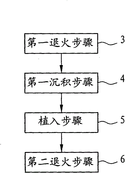
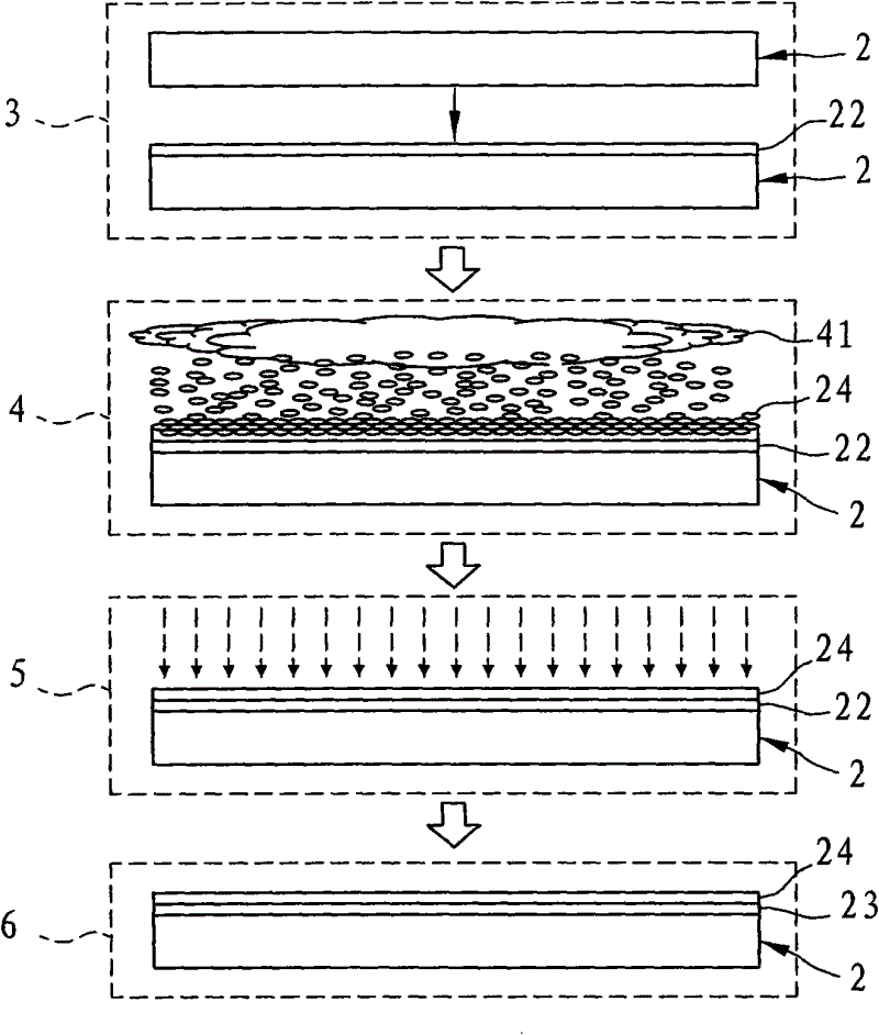
[0046] see figure 1 and figure 2 , is the first preferred embodiment of the wafer manufacturing method of the present invention, the first preferred embodiment includes a first annealing step 3, a first deposition step 4, an implantation step 5, and a second annealing step 6 .

[0047] It is worth mentioning that the wafer 2 used in the steps of this manufacturing method below generally refers to a wafer 2 with poor quality and many defects that is sliced ​​near the head and tail of the crystal column. ...


PUM


Abstract

The invention relates to a wafer suitable for a nanometer technology and a method for manufacturing the same. The manufacturing method comprises the following steps: a first annealing step, a first deposition step, an implantation step and a second annealing step. According to the first annealing step, annealing processing is carried out on a wafer at the temperature of over 650 DEG C so as to form a high-quality silicon layer on the surface of the wafer. According to the first deposition step, a silicon-germanium gas source is utilized to deposit a silicon-germanium deposition layer on the high-quality silicon layer of the wafer after the annealing processing. According to the implantation step, oxygen ions are implanted into the wafer. And according to the second annealing step, annealing processing is carried out on the wafer with implantation of the oxygen ions at the temperature of over 650 DEG C so as to form a silicon oxide layer. Therefore, it is easy to control uniformity and surface flatness of all material layers of the manufactured wafer and thus a wafer with nonuniform mass and low price can be manufactured into a wafer with uniform mass, so that the nanometer technology can be utilized conveniently.

Description

technical field [0001] The invention relates to a wafer and a manufacturing method thereof, in particular to a wafer and a manufacturing method that can be provided to semiconductor factories in the nanotechnology era. Background technique [0002] The wafers used in the existing semiconductor process are pulled out by Czochralski-grown crystal pillars, and then the crystal pillars are cut into sections and sliced ​​to produce wafers. Among the wafers cut out of the crystal column, the best quality is called single crystal wafer (Epi-Wafer) and production wafer (Prime Wafer). The "middle" section, and the wafers cut near the first and last sections have a higher proportion of defects and poorer quality, so they are usually sold at a low price and are used as control, blank and test wafers. Circle (with names like Test-Wafer or Dummy Wafer or Monitor Wafer). Test wafers are usually used for testing and experiments, and are difficult to use in normal processes, and the price...

Claims


Application Information

Patent Timeline
Patent Type & Authority Applications(China)
IPC IPC(8): H01L21/02H01L29/06
Inventor 陈柏颖
Owner 陈柏颖
Why Eureka
Try Eureka