Micro-nano integrated processing technology based three-dimensional anti-drag micro-channel structure and preparation method thereof

An integrated processing and micro-channel technology, applied in the field of micro-machining, can solve problems such as complex process, high cost, and inability to realize three-dimensional drag-reducing micro-channel, and achieve simple process, low cost, and improved uniformity and stability Effect

Inactive Publication Date: 2012-08-08
PEKING UNIV
View PDF5 Cites 6 Cited by
  • Summary
  • Abstract
  • Description
  • Claims
  • Application Information

AI Technical Summary

Problems solved by technology

[0005] In recent years, researchers have proposed a drag-reducing channel design based on surface modification of micro-nano dual-scale particles [Example: Lu Si, Chinese Science: Series G, 2010, 40: 916-924], which can achieve high-efficiency drag-reducing effects, However, the realization of the above-mentioned micro-nano dual-scale particle structure usually requires multi-step complex processes and high cost. More importantly, it is difficult to realize the drag-reducing structure on the sidewall and top surface of the groove, that is, it is impossible to realize the real three-dimensional drag-reducing microstructure. Runner

Method used


Image

  • Micro-nano integrated processing technology based three-dimensional anti-drag micro-channel structure and preparation method thereof
  • Micro-nano integrated processing technology based three-dimensional anti-drag micro-channel structure and preparation method thereof
  • Micro-nano integrated processing technology based three-dimensional anti-drag micro-channel structure and preparation method thereof

Examples


Embodiment Construction

[0034] Obviously, many modifications and changes made by those skilled in the art based on the gist of the present invention belong to the protection scope of the present invention.

[0035] In order to make the above objects, features and advantages of the present invention more comprehensible, the embodiments of the present invention will be further described in detail below in conjunction with the accompanying drawings and specific implementation methods.

[0036] Below in conjunction with accompanying drawing 1 to Figure 5 A three-dimensional drag-reducing microchannel structure based on micro-nano integrated processing technology provided by the present invention and the specific steps of its preparation method are described.

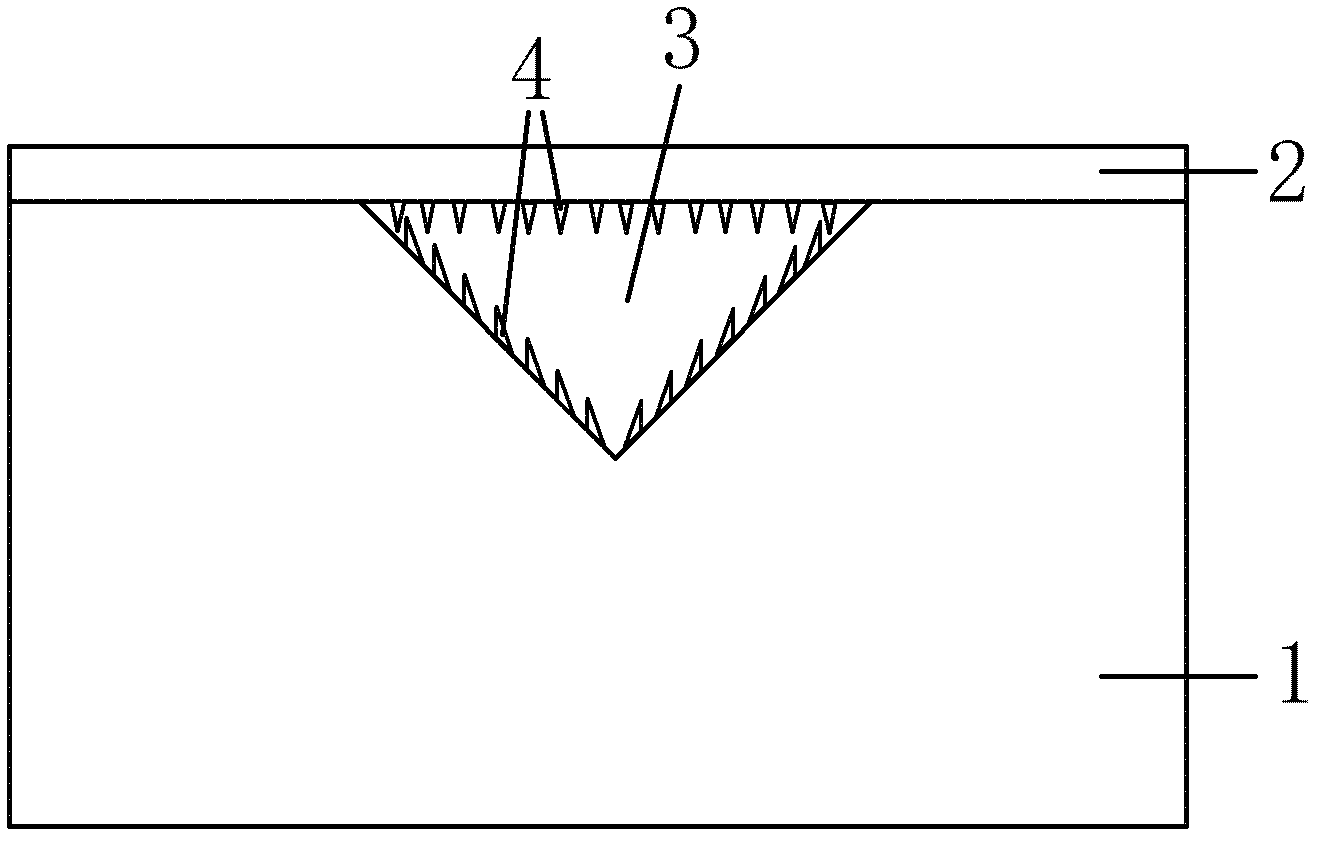
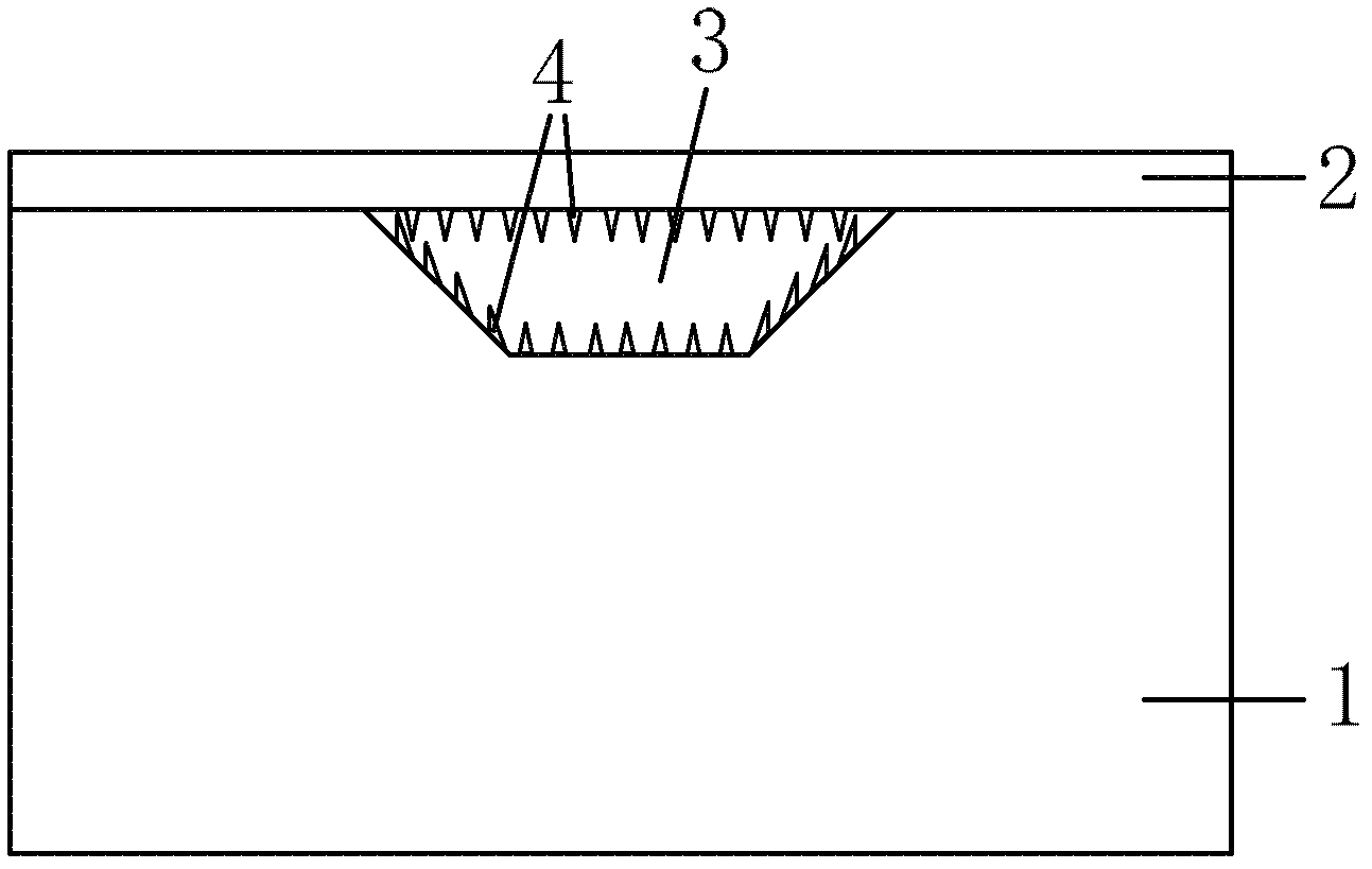
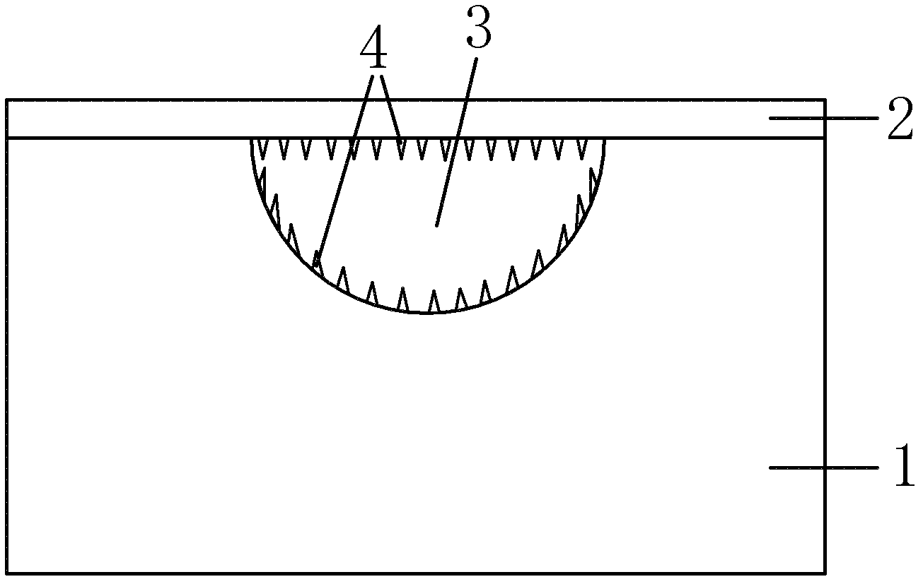
[0037] Referring to Figure 1, Figure 1(a) to Figure 1(b) It is a structural schematic diagram of a three-dimensional drag-reducing microfluidic channel based on micro-nano integrated processing technology of the present invention, and its cross-...


PUM

PropertyMeasurementUnit
thicknessaaaaaaaaaa
sizeaaaaaaaaaa
diameteraaaaaaaaaa

Abstract

The invention discloses a micro-nano integrated processing technology based three-dimensional anti-drag micro-channel structure and a preparation method thereof, relating to the technical field of micromachining. The preparation method comprises the steps of: directly preparing a high density and high aspect ratio nano dimension cone array on each surface of a silicon-based micron dimension groove by utilizing DRIE (Deep Reactive Ion Etching) without mask optimization to increase a superficial area to volume ratio; and depositing a layer of fluoro-based polymer on the surface of the silicon-based micron dimension groove at the same time to reduce a surface energy and realize a surface structure with super-hydrophobic properties, thereby further realizing a true three-dimensional anti-drag micro-channel structure. The micro-nano integrated processing technology based three-dimensional anti-drag micro-channel structure, disclosed by the invention, has the advantages that: the high density and high aspect ratio nano dimension cone array can be produced without damaging the original micron dimension structure; 100% coverage of a nano forest for the micron dimension groove can be realized and a true three-dimensional anti-drag micro-channel is thereby realized. The micro-nano integrated processing technology based three-dimensional anti-drag micro-channel structure can improve the area to volume ratio thereof extremely and reduce the surface energy to enable the surface of the micro-channel to have the super-hydrophobic properties, thereby realizing an excellent anti-drag effect. The micro-nano integrated processing technology based three-dimensional anti-drag micro-channel structure has simple technology, low cost and easy industrialization.

Description

technical field [0001] The invention relates to the technical field of micro-processing, in particular to a three-dimensional drag-reducing micro-channel structure and a preparation method based on micro-nano integrated processing technology. Background technique [0002] Microelectromechanical system (MEMS) refers to micromechanical basic components including micromechanical sensors and actuators produced by micromachining technology, as well as micro energy sources and high-performance electronic integrated circuits produced by integrated circuit processing technology. Microelectromechanical devices, devices or systems. Since its emergence in the 1980s, as an emerging, high-tech multi-field interdisciplinary subject, MEMS has attracted extensive attention from researchers at home and abroad, and is known as a new technological revolution leading the development of the microelectronics industry in the new century. After nearly 30 to 40 years of development, MEMS has achiev...

Claims


Application Information

Patent Timeline
Patent Type & Authority Applications(China)
IPC IPC(8): B81C1/00B01L3/00
Inventor 张海霞张晓升朱福运褚世敢
Owner PEKING UNIV
Why Eureka
Try Eureka