Method of protection treatment on millimeter-wave circuit component by use of vacuum vapor deposition membrane

A circuit component and vapor deposition technology, which is applied in the manufacture of circuits, electrical components, semiconductors/solid-state devices, etc., can solve the problems of complex hermetic packaging structure design, large component volume and weight, long manufacturing cycle, etc., and achieve lightweight , high reliability, weight reduction effect

Inactive Publication Date: 2012-08-15
10TH RES INST OF CETC
View PDF5 Cites 9 Cited by
  • Summary
  • Abstract
  • Description
  • Claims
  • Application Information

AI Technical Summary

Problems solved by technology

[0006] The purpose of the present invention is to solve the problems of large volume and weight and long design and manufacturing cycle caused by the hermetic package protection of millimeter wave circuit components, and to provide a method that does not need to use metal shell hermetic package, which can improve the combination of lead wires and solder joints. Strength, to ensure the long-ter...

Method used


Image

  • Method of protection treatment on millimeter-wave circuit component by use of vacuum vapor deposition membrane
  • Method of protection treatment on millimeter-wave circuit component by use of vacuum vapor deposition membrane
  • Method of protection treatment on millimeter-wave circuit component by use of vacuum vapor deposition membrane

Examples


Embodiment Construction

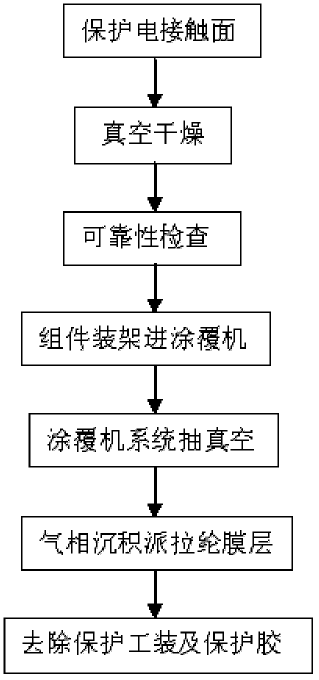
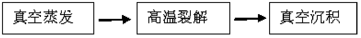
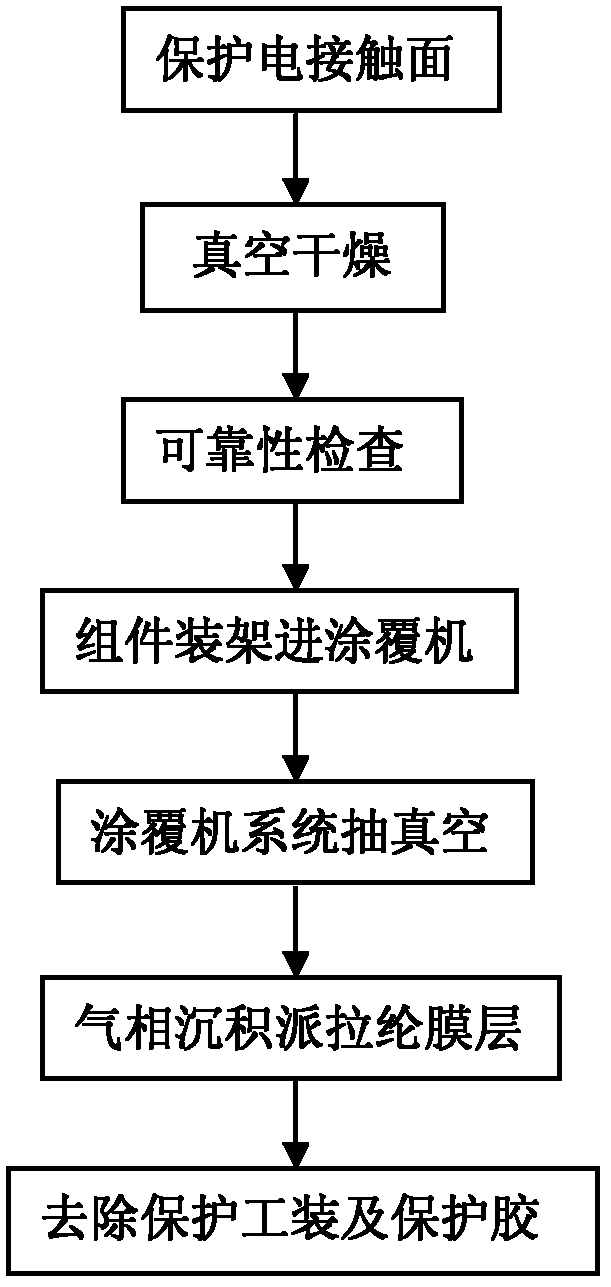
[0020] refer to figure 1 . In the manufacturing process of the millimeter wave circuit component, the protection treatment process of the present invention is usually added after the processing and performance debugging of the millimeter wave circuit component are completed. 1. Protect the electrical contact surface; 2. Vacuum drying; 3. Reliability inspection; 4. Mount the components into the coating machine; 5. Vacuumize the coating machine system; Protective tooling and protective glue. The main steps include:

[0021] a) In a clean environment, use protective tooling, pressure-sensitive tape or peelable glue to protect the unprotected parts (electrical contact surfaces) of the millimeter-wave circuit components that need to be protected;

[0022] b) Use a vacuum oven to vacuum-dry the millimeter-wave circuit components to be coated;

[0023] c) In a clean environment, use a 5x magnifying glass to check whether the mask protection of the electrical contact surface meets...


PUM

PropertyMeasurementUnit
Thicknessaaaaaaaaaa

Abstract

The invention provides a method of protection treatment on a millimeter-wave circuit component by use of a vacuum vapor deposition membrane. Through the method, the corrosion resistance and long-term work reliability of the millimeter-wave circuit component can be obviously improved, the volume and weight can be greatly reduced, and the protection treatment method adopting metal shell leaktight encapsulation is not needed. The method comprises the following steps of: putting the millimeter-wave circuit component subjected to partial protection treatment into a vacuum oven for vacuum drying treatment under clean environment; placing the millimeter-wave circuit component on a tool rack of a room-temperature vacuum deposition chamber of a coating machine, and sealing and vacuumizing the chamber; heating p-xylene ring dimer at 175 DEG C to sublimate into a gaseous state, and feeding into a splitting cavity of the coating machine so that the molecular bond of the xylene ring dimer is broken at 680 DEG C and the xylene ring dimer is split into a p-xylene monomer with reactivity; and feeding the p-xylene monomer into the room-temperature vacuum deposition chamber so that the p-xylene monomer deposits on the surface of the millimeter-wave circuit component and is polymerized to form a parylene film protection layer.

Description

technical field [0001] The invention relates to a protection method for millimeter wave circuit components. Background technique [0002] Modern electronic equipment is developing in the direction of short, small, light, thin, high reliability, high speed, high performance and low cost, especially airborne, ship-borne and space-borne electronic equipment, and portable electronic products have a large impact on volume and weight. The requirements for reliability and reliability are becoming more and more stringent. It is required to continuously increase the assembly and interconnection density of microwave circuits to achieve miniaturization, light weight and high reliability of microwave circuits. Higher requirements are put forward for microwave components and their micro-assembly technology. Therefore, multi-chip module technology has been widely researched and applied. [0003] Millimeter-wave circuit components with an operating frequency of around 35GHz include millim...

Claims


Application Information

Patent Timeline
IPC IPC(8): H01L21/56
Inventor 敖辽辉仝晓刚
Owner 10TH RES INST OF CETC
Why Eureka
Try Eureka