Supercharge Your Innovation With Domain-Expert AI Agents!

Forming a compound-nitride structure that includes a nucleation layer

A nitride, nitride layer technology, applied in the direction of coating, gaseous chemical plating, metal material coating process, etc. Problems such as the quality of the nitride layer

Inactive Publication Date: 2012-08-15
APPLIED MATERIALS INC
View PDF8 Cites 9 Cited by
  • Summary
  • Abstract
  • Description
  • Claims
  • Application Information

AI Technical Summary

Problems solved by technology

However, the quality of conventional Ill-nitrides is often unsatisfactory because the film properties (such as thickness, island density, island size) of the buffer layer are not always consistent
Any slight variation in the formation parameters during nucleation tends to affect the quality of the nitride layer, which in turn leads to distortion or dislocation of the nucleation islands prior to incorporation, thereby negatively affecting the formation of bulk III-nitrides

Method used


Image

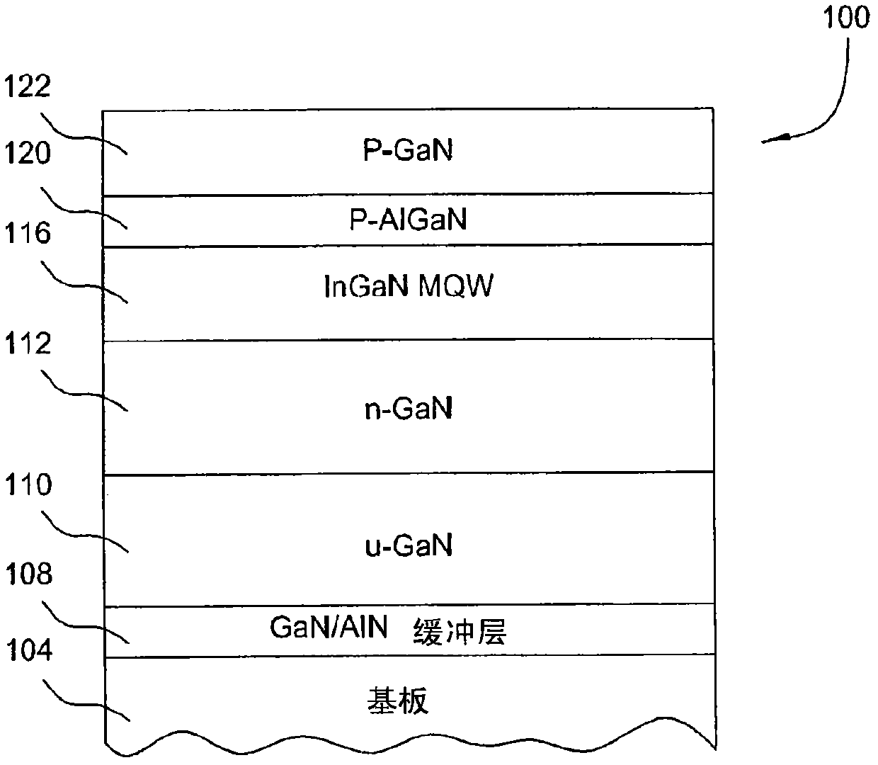
  • Forming a compound-nitride structure that includes a nucleation layer
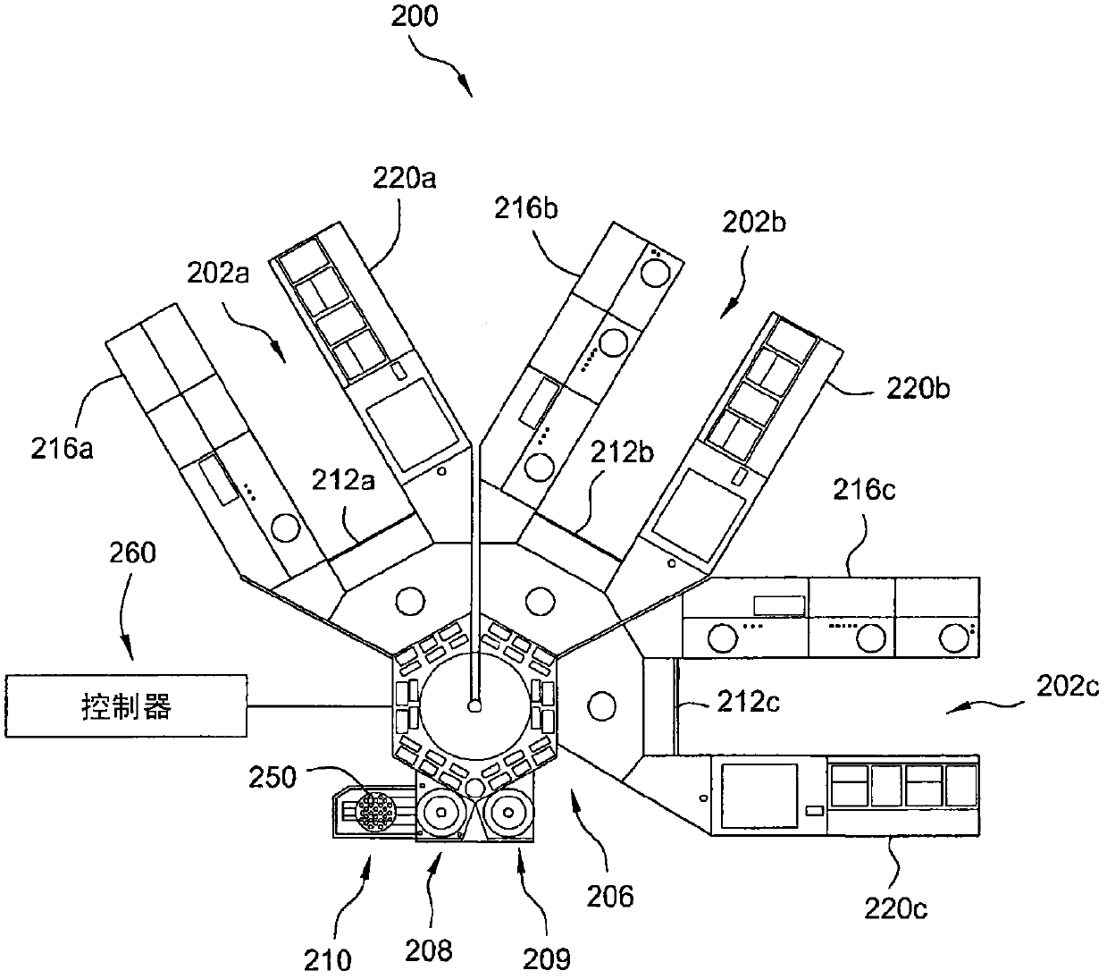
  • Forming a compound-nitride structure that includes a nucleation layer
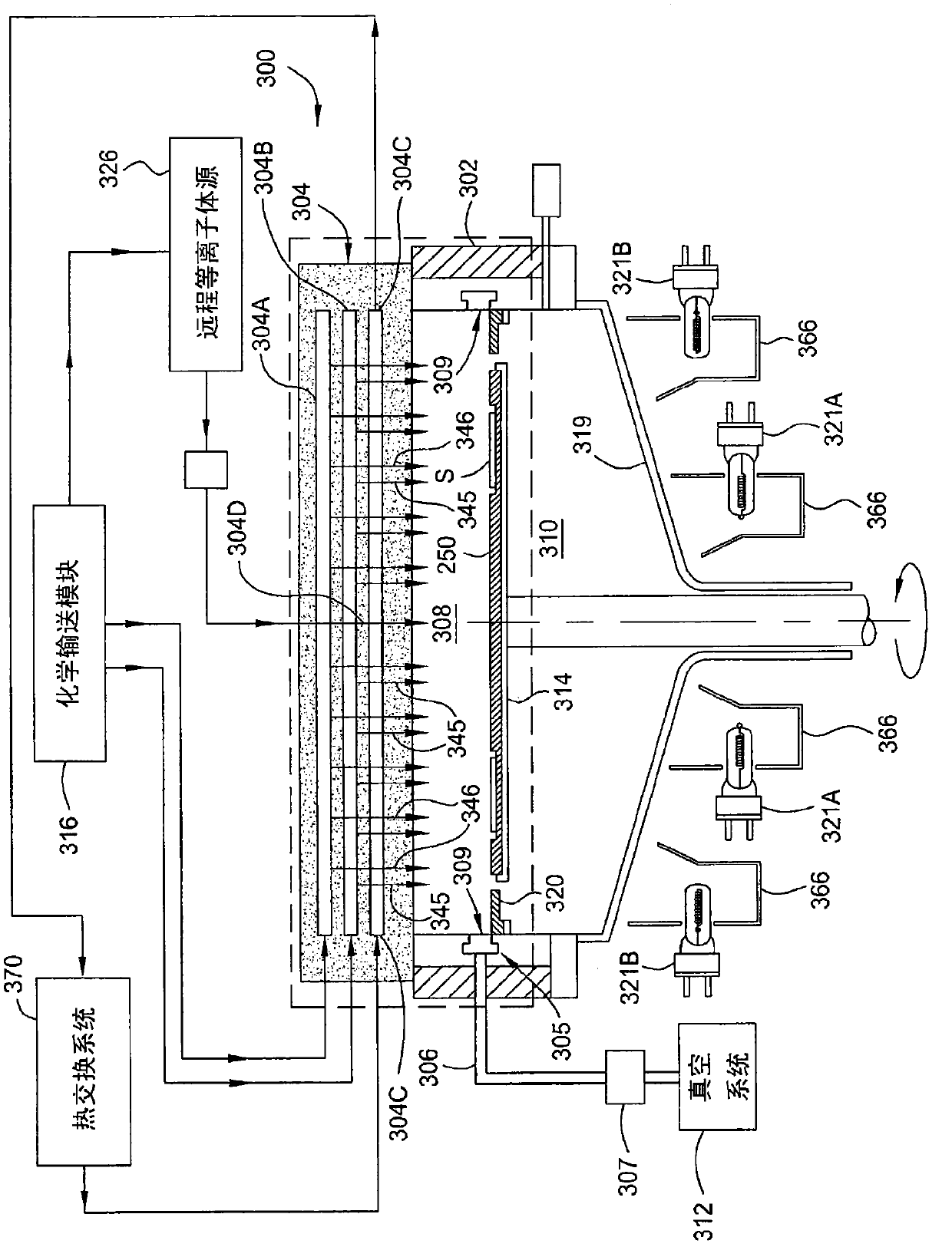
  • Forming a compound-nitride structure that includes a nucleation layer

Examples


Embodiment Construction

[0018] Embodiments of the invention described herein generally relate to the use of metal organic chemical vapor deposition (MOCVD), hydride vapor phase epitaxy (HVPE), physical vapor deposition (PVD), chemical vapor deposition (CVD) and / or atomic layer deposition ( ALD) processes to form III-V materials. In one embodiment where a sapphire substrate is selected, the growth of thick Ill-nitrides can be deposited in a HVPE or MOCVD chamber, while a separate process chamber (such as a PVD, MOCVD, CVD or ALD chamber) can be used at a lower A buffer layer (or sometimes called a nucleation layer) is grown on a sapphire substrate at a low growth rate. The buffer layer can be GaN, AlN, AlGaN, InGaN or InAlGaN, and can be doped or undoped.

[0019] In another embodiment where silicon-based substrates are chosen, the growth of thick Ill-nitrides can be deposited in a HVPE or MOCVD chamber in which an Al-free environment is provided, while a separate process chamber without a Ga environ...


PUM

PropertyMeasurementUnit
diameteraaaaaaaaaa
thicknessaaaaaaaaaa
thicknessaaaaaaaaaa

Abstract

The present invention generally provides apparatus and methods for forming LED structures. In one embodiment where a sapphire substrate is selected, the growth of bulk Group III-nitrides may be deposited in a HVPE or MOCVD chamber while a separate processing chamber, such as a PVD, MOCVD, CVD, or ALD chamber, may be used to grow buffer layers on the sapphire substrate at lower growth rate. The buffer layer may be GaN, AlN, AlGaN, InGaN, or InAlGaN. In another embodiment where a silicon-based substrate is selected, the growth of bulk Group III-nitrides may be deposited in a HVPE or MOCVD chamber in which an Al-free environment is provided while a separate processing chamber with a Ga-free environment is used to grow a Ga-free buffer layer, such as Al, AlN, or SiN, on the silicon-based substrate. The separate processing chamber may be a PVD, CVD, MOCVD, a plasma assisted MOCVD, or other vapor phase deposition techniques.

Description

technical field [0001] Embodiments of the present invention relate generally to the fabrication of components such as light emitting diodes (LEDs), laser diodes (LDs), and more particularly to processes for forming III-V materials. Background technique [0002] Group III-V materials are finding increasing importance in the development and fabrication of various semiconductor components such as short-wavelength LEDs, LDs, and electronic components including high power, high frequency and high temperature transistors and integrated circuits. For example, short-wavelength (eg, blue / green to ultraviolet) LEDs are fabricated using the III-nitride semiconductor material gallium nitride (GaN). It has been found that short-wavelength LEDs fabricated with GaN provide significantly higher efficiencies and longer operating times than short-wavelength LEDs fabricated with non-nitride semiconductor materials, including group II-VI elements. [0003] One method that has been used to depo...

Claims


Application Information

Patent Timeline
Patent Type & Authority Applications(China)
IPC IPC(8): H01L21/20H01L33/00
CPCC23C16/301C23C16/303C23C16/54H01L21/0237H01L21/02458H01L21/02505H01L21/0254H01L21/0262H01L33/007H01L33/00
Inventor 苏杰
Owner APPLIED MATERIALS INC
Features
  • R&D
  • Intellectual Property
  • Life Sciences
  • Materials
  • Tech Scout
  • Unparalleled Data Quality
  • Higher Quality Content
  • 60% Fewer Hallucinations
Learn More