

Preparation method of nitrogen-doped tin dioxide film
A tin dioxide and nitrogen doping technology, applied in cable/conductor manufacturing, conductive layer on insulating carrier, ion implantation plating, etc. The effect of extensive, simple and easy-to-control preparation process
- Summary
- Abstract
- Description
- Claims
- Application Information
AI Technical Summary
Problems solved by technology
Method used
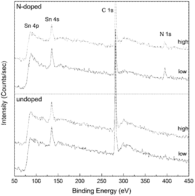
Image


Examples
Embodiment 1
[0024] Clean the glass substrate, dry it with nitrogen, put it into the sample stage, and install it in the sputtering chamber of the magnetron sputtering apparatus;
[0025] ●Evacuate the vacuum chamber 6×10 -4 Pa, according to a certain volume ratio O: N = 1:99 into O 2 (purity 99.99%) and N 2 (purity 99.99%) mixed gas, control the air pressure in the sputtering chamber at 5Pa;
[0026] ●Turn on the RF power supply and the filament switch to start the glow, the incident power is 120W, and the sputtering pressure is 1.5Pa;
[0027] ●Pre-sputter the substrate for 30 minutes, and adjust the substrate heating temperature to 400°C;
[0028] Thin film deposition: the sputtering rate is 10-12nm / min, the time is controlled at 30min; the film thickness is 300nm
[0029] Annealing after film deposition: keep warm for 20 minutes at 400°C in an oxidizing atmosphere;
[0030] The resistivity of 2.0×10 can be obtained -3 Ω·cm, visible light transmittance 77%, stable performance, tra...
Embodiment 2
[0032] 1) Clean the glass substrate, dry it with nitrogen, put it into the sample stage, and install it in the sputtering chamber of the magnetron sputtering apparatus;
[0033] 2) Vacuum the vacuum chamber to 6×10 -4 Pa, according to a certain volume ratio O: N = 3:97 into O 2 (purity 99.99%) and N 2 (purity 99.99%) mixed gas, control the air pressure in the sputtering chamber at 5Pa;
[0034] 3) Turn on the RF power supply and the filament switch to start the glow, the incident power is 100W, and the sputtering pressure is 1.5Pa;
[0035] 4) Perform pre-sputtering on the substrate for 30 minutes, and adjust the heating temperature of the substrate to 400°C;
[0036] 5) Thin film deposition: the sputtering rate is 8-10nm / min, the time is controlled at 25min; the film thickness is 200nm
[0037] 6) Annealing after film deposition: keep warm for 40 minutes at 500°C in an oxidizing atmosphere;
[0038] The resistivity of 2.4×10 can be obtained -3 Ω·cm, visible light transm...
Embodiment 3
[0040] 1) Clean the glass substrate, dry it with nitrogen, put it into the sample stage, and install it in the sputtering chamber of the magnetron sputtering apparatus;
[0041] 2) Vacuum the vacuum chamber to 6×10 -4 Pa, according to a certain volume ratio O:N=6:94 into O 2 (purity 99.99%) and N 2 (purity 99.99%) mixed gas, control the air pressure in the sputtering chamber at 5Pa;
[0042] 3) Turn on the RF power supply and the filament switch to start the glow, the incident power is 150W, and the sputtering pressure is 1.5Pa;
[0043] 4) Perform pre-sputtering on the substrate for 30 minutes, and adjust the heating temperature of the substrate to 400°C;
[0044] 5) Thin film deposition: the sputtering rate is 10-15nm / min, and the time is controlled at 10min; the film thickness is 100nm
[0045] 6) Annealing after film deposition: keep warm for 60 minutes at 400°C in an oxidizing atmosphere;
[0046] The resistivity of 8.2×10 can be obtained -3 Ω·cm, visible light tran...
PUM
| Property | Measurement | Unit |
|---|---|---|
| Thickness | aaaaa | aaaaa |
| Resistivity | aaaaa | aaaaa |
| Thickness | aaaaa | aaaaa |
Abstract
Description
Claims
Application Information