Double-junction GaAs lamination laser photovoltaic cell and fabrication method thereof
A laser photovoltaic cell and lamination technology, applied in photovoltaic power generation, circuits, electrical components, etc., can solve problems such as power failure, and achieve the effects of improving battery efficiency, reducing losses, and saving process time.
- Summary
- Abstract
- Description
- Claims
- Application Information
AI Technical Summary
Problems solved by technology
Method used
Image
Examples
no. 1 Embodiment approach
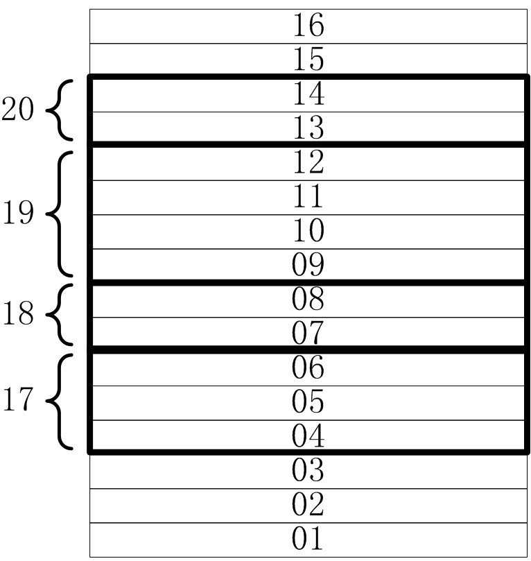
[0026] figure 1 It is a schematic cross-sectional view of the first embodiment of the double-junction GaAs stacked laser photovoltaic cell.
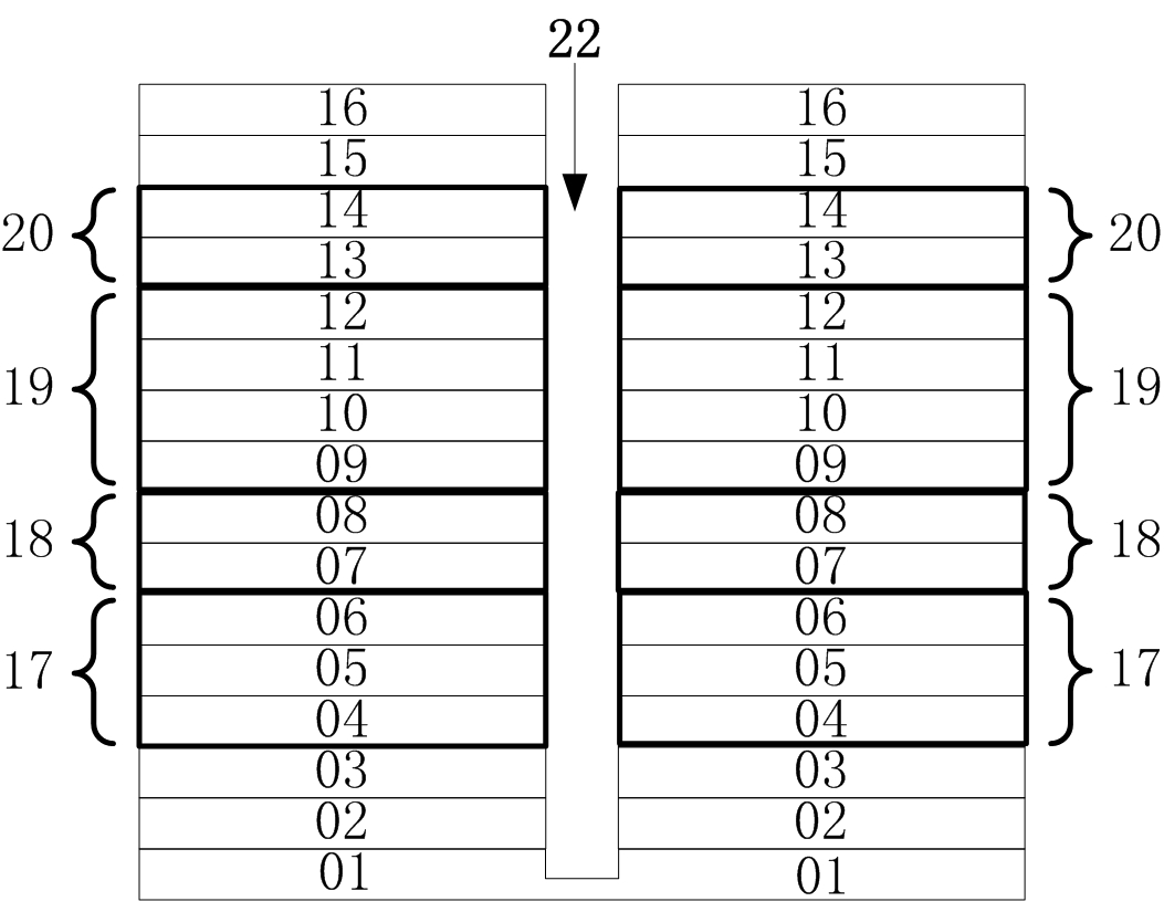
[0027] figure 2 It is a schematic cross-sectional view of the isolation groove structure of the first embodiment of the double-junction GaAs stacked laser photovoltaic cell.
[0028] This embodiment provides a double-junction GaAs laminated laser photovoltaic cell, including a semi-insulating GaAs substrate 01, and an N-type GaAs conductive layer 02, a first tunnel junction 17, and a bottom substrate 01 grown sequentially on the substrate 01. Cell 18 , second tunnel junction 19 , top cell 20 , window layer 15 and GaAs contact layer 16 .
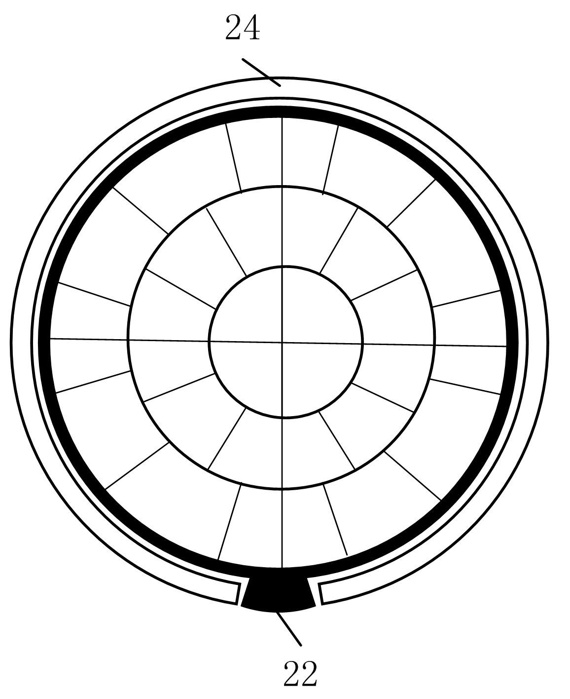
[0029] The double-junction GaAs laminated laser photovoltaic cell further includes an isolation groove 22, the isolation groove 22 penetrates from the GaAs contact layer 16 to the substrate 01 until the substrate 01 is exposed, and the isolation groove 22 is filled with Silicon oxide or polyimide gl...
no. 2 Embodiment approach
[0048] Prepare the structure as figure 1 The double-junction GaAs laminated laser photovoltaic cell comprises the steps of:
[0049] (1) growing an N-type GaAs conductive layer 02 on a semi-insulating GaAs substrate 01;
[0050] (2) growing an N-type AlGaAs ((Al)GaInP) third barrier layer 03 on the N-type GaAs conductive layer 02;
[0051] (3) On the third barrier layer 03, the N-type doping concentration is greater than 1×10 19 cm -3 The first GaAs (Ga 0.51 In 0.49 P) layer 04, the re-growth P-type doping concentration is greater than 1×10 19 cm -3 the first (Al)GaAs layer 05 to form a first tunnel junction 17;
[0052] (4) growing a P-type AlGaAs ((Al)GaInP) first barrier layer 06 of the first tunnel junction 17 on the first (Al)GaAs layer 05, which can also be used as the back field layer of the bottom cell 18;
[0053] (5) Growing the first P region 07 of the P-type GaAs absorption layer on the above-mentioned first barrier layer 06, and growing the first N region ...
PUM
 Abstract
Description
Claims
Application Information


