Amorphous-oxide thin-film transistor, manufacturing method thereof, and display panel

A technology of amorphous oxide and thin film transistors, which is applied in the direction of transistors, semiconductor/solid-state device manufacturing, semiconductor devices, etc., can solve the problems of reduced current drive capability, low threshold voltage, and increased parasitic resistance of source and drain, and achieve improved Driving capability and effect of reduction in parasitic resistance

Active Publication Date: 2012-09-05
BOE TECH GRP CO LTD
View PDF4 Cites 33 Cited by
  • Summary
  • Abstract
  • Description
  • Claims
  • Application Information

AI Technical Summary

Problems solved by technology

However, the semiconductor channel generated by amorphous oxide often has a very high carrier concentration, so that the threshold voltage becomes very low or even falls to a negative value (for n-type devices), that is, when the gate is biased at zero , the device

Method used


Image

  • Amorphous-oxide thin-film transistor, manufacturing method thereof, and display panel
  • Amorphous-oxide thin-film transistor, manufacturing method thereof, and display panel
  • Amorphous-oxide thin-film transistor, manufacturing method thereof, and display panel

Examples


Embodiment 1

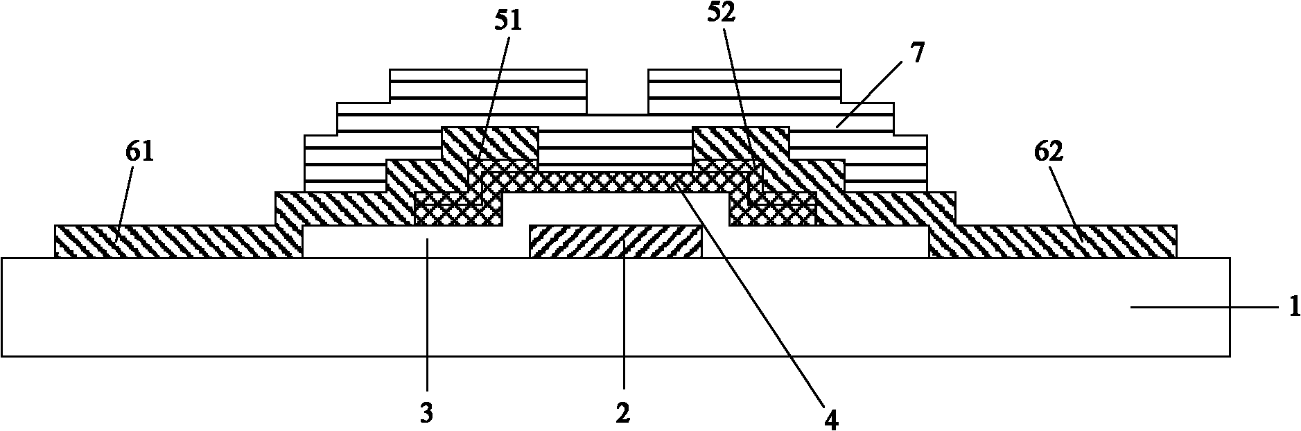
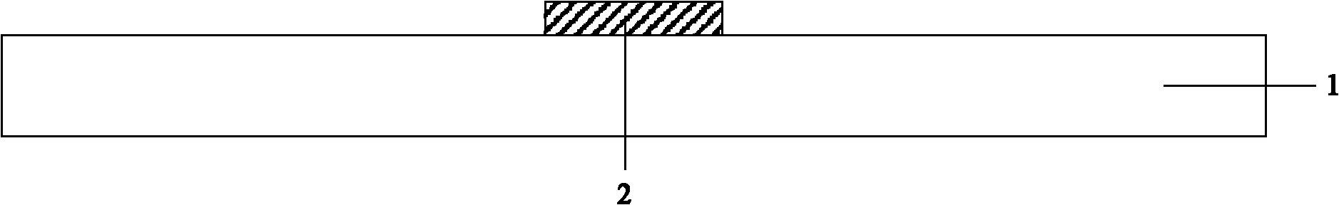
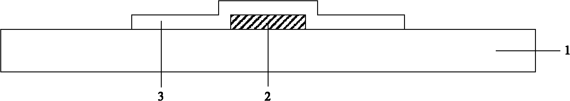
[0036] Such as figure 1 As shown, the embodiment of the present invention provides an amorphous oxide thin film transistor, including: a gate 2, a gate insulating layer 3, a semiconductor active layer, a source 61, a drain 62 and a passivation protection layer 7, the The semiconductor active layer is a double-layer structure of a channel layer 4 and an ohmic contact layer, and the channel layer 4 has a higher oxygen content than the ohmic contact layer;

[0037] The channel layer 4 is bonded to the gate insulating layer 3, the ohmic contact layer is divided into two independent ohmic contact regions 51, 52, and the two independent ohmic contact regions 51, 52 are respectively connected to The source electrode 61 and the drain electrode 62 are bonded together.

[0038] Wherein, the channel layer 4 is formed by sputtering an amorphous oxide material in an oxygen-containing atmosphere; the ohmic contact layer is formed by sputtering an amorphous oxide material in an oxygen-free ...

Embodiment 2

[0088] like Figure 13 As shown, the embodiment of the present invention provides an amorphous oxide thin film transistor, including: a gate 2, a gate insulating layer 3, a semiconductor active layer, a source 61, a drain 62 and a passivation protection layer 7, the The semiconductor active layer is a double-layer structure of a channel layer 4 and an ohmic contact layer, and the channel layer 4 has a higher oxygen content than the ohmic contact layer;

[0089] The channel layer 4 is bonded to the gate insulating layer 3, the ohmic contact layer is divided into two independent ohmic contact regions 51, 52, and the two independent ohmic contact regions 51, 52 are respectively connected to The source electrode 61 and the drain electrode 62 are bonded together;

[0090] An etching protection layer 9 is formed between the two independent ohmic contact regions 51 , 52 , and the etching protection layer 9 is located between the channel layer 4 and the passivation protection layer 7...


PUM


Abstract

The embodiment of the invention discloses an amorphous-oxide thin-film transistor, a manufacturing method thereof, and a display panel, relates to the field of design and manufacture of the thin-film transistor and the display panel, which are used for reducing parasitic resistance of a source and a drain. The amorphous-oxide thin-film transistor is characterized in that the substrate comprises a grid electrode, a grid insulating layer, a semiconductor active layer, a source electrode, a drain electrode and a passivation protecting layer, wherein the semiconductor active layer is of a two-layer structure with a channel layer and an ohmic contact layer, and the oxygen content of the channel layer is higher than that of the ohmic contact layer; and in addition, the channel layer and the ohmic contact layer are attached, and the ohmic contact layer is divided into two independent ohmic contact areas which are respectively attached with the source electrode and the drain electrode.

Description

technical field [0001] The invention relates to the field of design and preparation of thin film transistors, in particular to an amorphous oxide thin film transistor, a manufacturing method thereof, and a display panel. Background technique [0002] At present, thin film transistors (TFTs) widely used in the field of liquid crystal display mainly include amorphous silicon thin film transistors and polysilicon thin film transistors. Among them, hydrogenated amorphous silicon (a-Si:H) thin film transistors have become the mainstream technology in the active matrix flat panel display industry due to their advantages such as simple preparation process and good backplane uniformity; however, they have defects such as low mobility and poor stability. It is rarely used in the field of large-area AMOLED (Active Matrix Organic Light Emitting Diode, active matrix organic light emitting diode). In addition, compared with amorphous silicon thin film transistors, polysilicon thin film ...

Claims


Application Information

Patent Timeline
IPC IPC(8): H01L29/06H01L29/36H01L29/04H01L29/786G02F1/1362G02F1/1368H01L21/336
CPCH01L29/78693H01L21/02565H01L21/02592H01L21/02631H01L21/0273H01L21/441H01L21/467H01L21/477H01L29/66969H01L29/78618
Inventor 刘晓娣孙力陈海晶
Owner BOE TECH GRP CO LTD
Why Eureka
Try Eureka