A superconducting field effect transistor, its manufacturing method and application method

A fabrication method and technology for transistors, applied in semiconductor/solid-state device manufacturing, semiconductor devices, electrical components, etc., can solve problems such as device leakage, transistor performance degradation, and difficulty in further reducing channel length, achieving high speed and improving stability. , the effect of avoiding device failure

Active Publication Date: 2016-04-06
肖德元
View PDF5 Cites 0 Cited by
  • Summary
  • Abstract
  • Description
  • Claims
  • Application Information

AI Technical Summary

Problems solved by technology

[0005] In view of the shortcomings of the prior art described above, the purpose of the present invention is to provide a superconducting field effect transistor, its manufacturing method and its application method, which are used to solve the problem that the channel length of superconducti

Method used


Image

  • A superconducting field effect transistor, its manufacturing method and application method
  • A superconducting field effect transistor, its manufacturing method and application method
  • A superconducting field effect transistor, its manufacturing method and application method

Examples


Embodiment 1

[0058] like Figure 4~Figure 10 Shown, the present invention provides a kind of manufacturing method of superconducting field effect transistor, and described manufacturing method comprises at least:

[0059] like Figure 4 As shown, step 1) is first performed to provide a semiconductor-on-insulator substrate, including a back substrate 701 , an insulating layer 702 on the back substrate 701 , and a semiconductor thin film of the first doped conductivity type on the insulating layer 702 .

[0060] In the method for manufacturing a superconducting field effect transistor, the semiconductor film is P-type doped or N-type doped Si, Ge, SiGe, SiGeC, or III-V semiconductor material. In this embodiment, the back substrate 701 is Si, and the insulating layer 702 is SiO 2 , the semiconductor film is N-type doped Si.

[0061] like Figure 5 As shown, then proceed to step 2), define a channel region 703 in the semiconductor film, and etch both sides of the channel region 703 to the ...

Embodiment 2

[0074] see Figure 4~Figure 10 , the present embodiment provides a manufacturing method of a superconducting field effect transistor, the basic steps of which are as in embodiment 1, wherein the semiconductor thin film is P-type doped, and the superconductor source 704 and superconductor drain 705 are P Type La-Sr-Cu-O, Y-Ba-Cu-O, Bi-Sr-Ca-Cu-O or Tl-Ba-Sr-Cu-O based superconducting thin films. Of course, in other embodiments, the superconducting thin film can also be any expected superconducting material. The channel region 703 is made of P-type doped Ge material, the shape of the channel region 703 is truncated, and the length is 50nm.

Embodiment 3

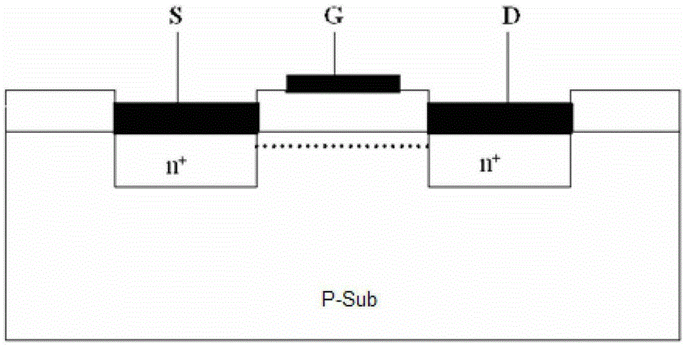
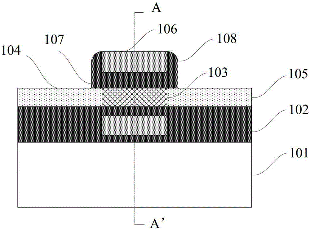
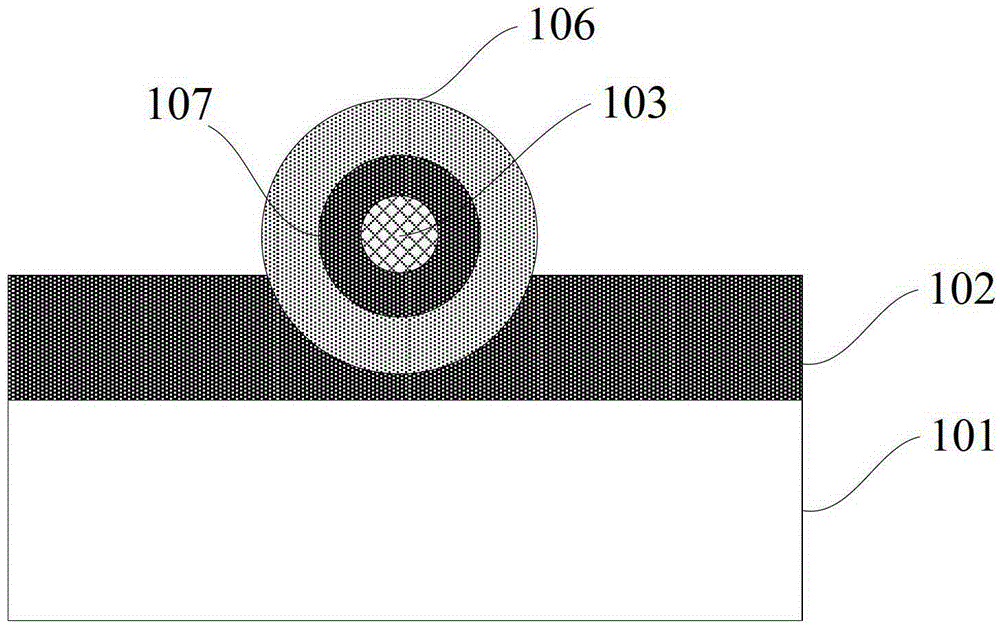
[0076] like Figure 2a~3e As shown, the present invention also provides a superconducting field effect transistor, comprising at least: a semiconductor-on-insulator substrate, a superconductor source 104 formed on the semiconductor-on-insulator substrate, a superconductor drain 105, and a superconductor source located at the superconductor source The channel region 103 between the electrode 104 and the superconductor drain 105, and the gate structure, wherein the channel region 103, the superconductor source 104, and the superconductor drain 105 have the same doping conductivity type.

[0077] The length of the channel region 103 is 10-1000nm. In the present embodiment, the length of the channel region 103 is 100nm, which is connected to the superconductor source and drain to be in a superconducting state, which greatly improves the performance of the device. drive current and response speed.

[0078] The channel region 103 is a column, prism, circular truncated or truncated ...


PUM

PropertyMeasurementUnit
Lengthaaaaaaaaaa
Lengthaaaaaaaaaa

Abstract

The invention provides a superconductive field effect transistor as well as a manufacturing method and an application method thereof. A superconductor source electrode, a superconductor drain electrode, a channel region and a grid electrode structure are formed on a semiconductor substrate on an insulator, wherein the channel region is located between the superconductor source electrode and the superconductor drain electrode; and the channel region, the superconductor source electrode and the superconductor drain electrode are the same in doping conducting types. A positive voltage or a negative voltage can be applied to the grid electrode structure through control so as to control on or off of the superconductive field effect transistor. With the adoption of the superconductive field effect transistor, working of nanoscale short channel devices can be realized, the problem of failure of nanoscale short channel inversion devices caused by increasing leakage current of the devices because source drain impurity ions diffuse to a channel is avoided at the same time, and the reliability of the devices is improved. Superconductivity of a semiconductor channel can be realized by using shorter channels, thus the response speed of the devices is greatly quickened.. The superconductive field effect transistor has the characteristics of large current, strong driving force, high speed, rapid response and simplicity in preparing process and is suitable for industrial production.

Description

technical field [0001] The invention belongs to the field of semiconductors, and in particular relates to a superconducting field effect transistor, a manufacturing method and an application method thereof. Background technique [0002] Superconducting field effect transistor, SuperconductorFET (SFET): It is an insulated gate field effect transistor that uses a superconducting channel to conduct electricity. Its source and drain electrode contact metals are superconductors (see illustration). Since the coherence length of the superconductor—the correlation length between the superconducting electron pairs (the spatial length of the correlation effect) is about 1nm to 100nm (within this length, there can be many superconducting electron pairs), the normal contact with the superconductor Conductor or semiconducting thin films will also become superconducting. Therefore, for a shorter device channel, it can also become a superconducting state, so this superconducting field ef...

Claims


Application Information

Patent Timeline
IPC IPC(8): H01L21/336H01L29/36H01L29/78
Inventor 肖德元
Owner 肖德元
Why Eureka
Try Eureka