

Plasma excimer nanometer laser
A nano-laser and plasmon technology, applied in nano-optics, nano-technology, nano-technology, etc., can solve the problems of plasmon leakage, limited application, and high laser threshold, and achieve the effect of reducing leakage and improving quality factor
- Summary
- Abstract
- Description
- Claims
- Application Information
AI Technical Summary
Problems solved by technology
Method used
Image

Examples
Embodiment 1
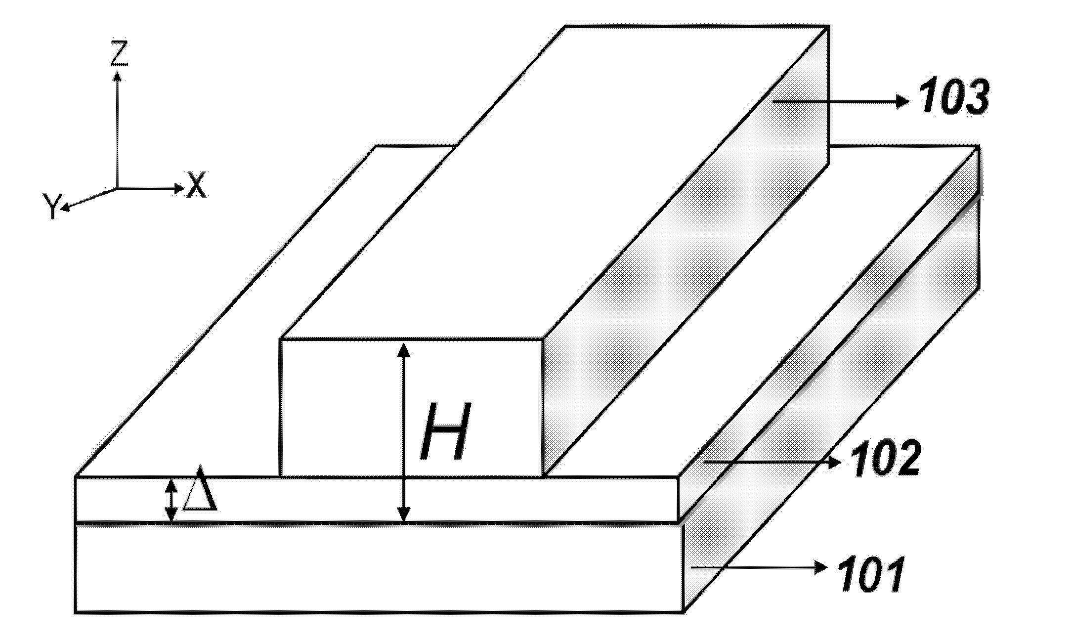
[0040] figure 1 Shown is the gain waveguide structure of Embodiment 1 of a plasmonic nanolaser provided by the present invention. Where x, y and z represent the coordinate axes x-axis, y-axis and z-axis respectively.
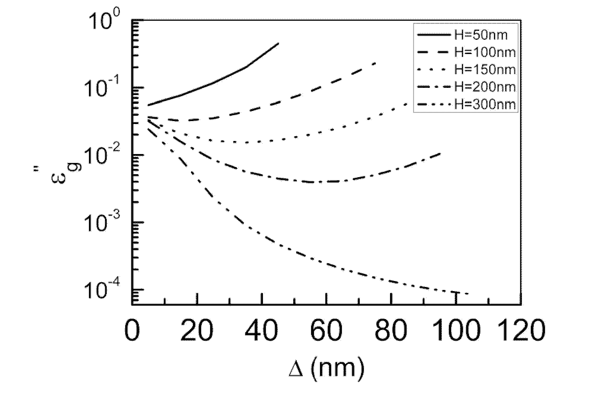
[0041] Embodiment 1 of the present invention provides a gain waveguide structure corresponding to a plasmonic nanolaser, including a first dielectric layer 101, a first isolation layer 102, and a gain medium cavity 103, and the first isolation layer 102 is placed in On the exposed surface of the first dielectric layer 101, the gain medium cavity 103 is placed on the exposed surface of the first isolation layer 102, the ratio range of the thickness of the first isolation layer 102 to the longitudinal thickness of the gain medium cavity 103 is less than 0.5, The plasmon oscillation heat loss of the first dielectric layer 101 is reduced, thereby reducing the threshold value of laser light, obtaining a suitable thick gain medium cavity 103, and laying a foundation ...
Embodiment 2
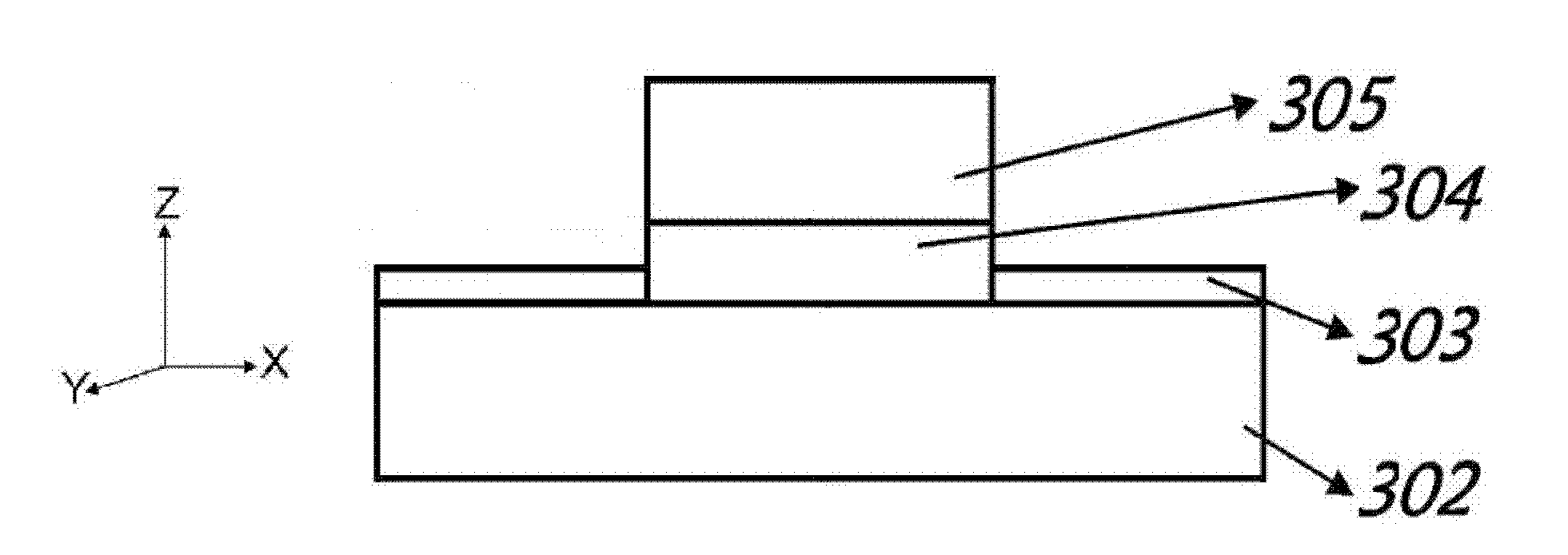
[0056] Figure 3A Shown is a cross-sectional structure diagram of Embodiment 2 of a plasmonic nanolaser provided by the present invention. Where x, y and z represent the coordinate axes x-axis, y-axis and z-axis respectively.
[0057] Embodiment 2 of the present invention provides a plasmonic nanolaser, including a first dielectric layer 302, a first isolation layer 304, and a gain medium cavity 305, and the first isolation layer 304 is placed on the first dielectric layer 302 The gain medium cavity 305 is placed on the exposed surface of the first isolation layer 304, and the ratio range of the thickness of the first isolation layer 304 to the longitudinal thickness of the gain medium cavity 305 is less than 0.5, so that the first dielectric layer The plasmon oscillation heat loss of 302 is small, thereby reducing the threshold value of the laser, obtaining a suitable thickness of the thicker gain medium cavity 305, and laying the foundation for further realizing the electro...
Embodiment 3
[0064] Figure 5 Shown is the cross-section and horizontal cross-section structure of Embodiment 3 of a plasmonic nanolaser provided by the present invention.
[0065] In the figure, x, y and z represent the coordinate axes x-axis, y-axis and z-axis respectively; the far right in the figure is the horizontal cross-sectional structure of the laser in the third embodiment; the middle of the figure is the cross-section of the third embodiment.
[0066] Embodiment 3 of the present invention provides a plasmonic nanolaser, including a first dielectric layer 502, a first isolation layer 504, and a gain medium cavity 505, and the first isolation layer 504 is placed on the first dielectric layer 502 On the exposed surface of the gain medium cavity 505 is placed on the exposed surface of the first isolation layer 504, the ratio range of the thickness h3 of the first isolation layer 504 to the longitudinal thickness h1 of the gain medium cavity 505 is less than 0.5, embodiment three Fu...
PUM
| Property | Measurement | Unit |
|---|---|---|
| Thickness | aaaaa | aaaaa |
| Thickness | aaaaa | aaaaa |
| Thickness | aaaaa | aaaaa |
Abstract
Description
Claims
Application Information