An organic semiconductor micro-nanocrystalline array, a preparation method thereof and application thereof in a photovoltaic cell

A technology of organic semiconductors and organic semiconductor layers, which is applied in semiconductor/solid-state device manufacturing, photovoltaic power generation, semiconductor devices, etc., and can solve problems such as low mobility, inability to be widely used in practical applications, short-circuit of thin-film devices, etc.

Active Publication Date: 2012-09-26
CHANGCHUN INST OF APPLIED CHEMISTRY - CHINESE ACAD OF SCI
View PDF5 Cites 8 Cited by
  • Summary
  • Abstract
  • Description
  • Claims
  • Application Information

AI Technical Summary

Problems solved by technology

However, due to the need for carrier gas transportation and precise control of the carrier gas flow rate, the cost is high and the experimental repeatability is poor.
In addition, due to the low substrate temperature (generally below 50°C), the grain size of the thin film is small and the mobility is low, which limits the further improvement of device performance.
[0003] On the other hand, researchers tried to increase the substrate temperature during deposition of organic small molecule f

Method used


Image

  • An organic semiconductor micro-nanocrystalline array, a preparation method thereof and application thereof in a photovoltaic cell
  • An organic semiconductor micro-nanocrystalline array, a preparation method thereof and application thereof in a photovoltaic cell
  • An organic semiconductor micro-nanocrystalline array, a preparation method thereof and application thereof in a photovoltaic cell

Examples


Embodiment 1

[0121] The preparation method of the organic semiconductor micro-nano crystal array of the present invention

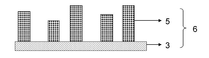
[0122] (I) if figure 1 The method for making the first organic semiconductor micro-nano crystal array 6 of the present invention shown is as follows:

[0123] (1) The substrate is indium tin oxide (ITO) glass, and the root mean square roughness (RMS) of the surface of the substrate used is less than 1nm, so it does not need to be smooth and can be used directly; or, the root mean square roughness (RMS) of the substrate surface ) greater than 1nm, the substrate is smoothed with an aqueous dispersion (PEDOT:PSS) of poly(3,4-ethylenedioxythiophene) poly(styrene sulfonate);

[0124] (2) vacuum-depositing the induction layer 3 on the surface of the substrate or the smoothed substrate;

[0125] The material of the induction layer 3 is P4T or BP2T, and the thickness is not less than 2 nanometers and not more than 12 nanometers;

[0126] (3) Vacuum deposition of an organic...

Embodiment 2

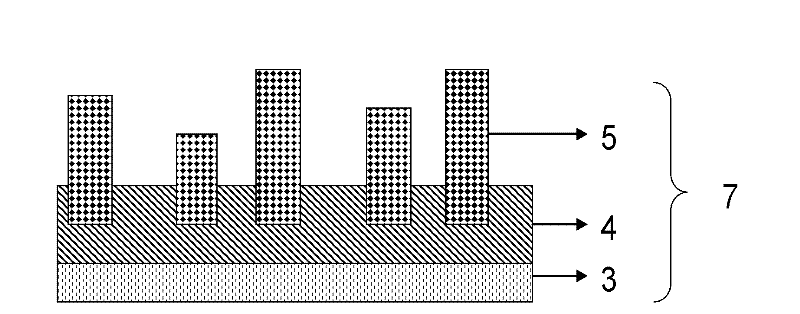
[0170] First structure of the present invention (as Figure 13 Shown) the preparation method of the photovoltaic cell containing organic semiconductor micro-nano crystal array is as follows:

[0171] (1) The substrate is ITO glass, and the root mean square roughness (RMS) of the substrate surface used is less than 1nm, so it does not need to be smoothed and used directly; or, the root mean square roughness (RMS) of the substrate surface is greater than 1nm, and PEDOT is used :PSS smoothing;

[0172] (2) Vacuum deposit an induction layer 3 on the surface of the substrate; the thickness of the induction layer 3 is not less than 2 nanometers and not more than 12 nanometers, and the material is BP2T or P4T;

[0173] (3) Vacuum deposit organic semiconductor micro-nano crystal layer 5 on the surface of induction layer 3, induction layer 3 and organic semiconductor micro-nano crystal layer 5 form micro-nano crystal array 6; The height of nanocrystalline grains is not less than 5 na...

Embodiment 3

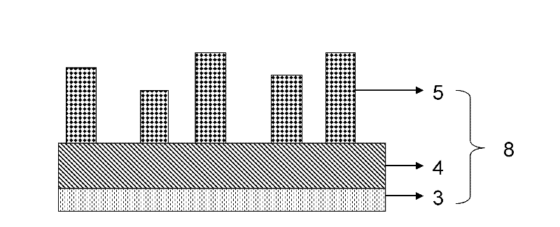
[0190] The second method of making photovoltaic cells containing organic semiconductor micro-nano crystal arrays of the present invention is as follows:

[0191] (1) The substrate is ITO glass, and the root mean square roughness (RMS) of the surface of the substrate used is less than 1nm, so it does not need to be smoothed, and it can be used directly; or, the root mean square roughness (RMS) of the substrate surface is greater than 1nm, use PEDOT :PSS smoothing;

[0192] (2) Vacuum deposit an induction layer 3 on the surface of the substrate; the thickness of the induction layer 3 is not less than 2 nanometers and not more than 12 nanometers, and the material is BP2T;

[0193] (3) p-type organic semiconductor layer 4 with a thickness of m is vacuum-deposited on the surface of induction layer 3, then vacuum co-deposited p-type organic semiconductor layer 4 and organic semiconductor micro-nano crystal layer 5, the organic semiconductor layer 4 of co-deposition The thickness is...


PUM

PropertyMeasurementUnit
Thicknessaaaaaaaaaa
Thicknessaaaaaaaaaa
Thicknessaaaaaaaaaa

Abstract

The invention provides an organic semiconductor micro-nanocrystalline array, a preparation method thereof and application thereof in a photovoltaic cell. Based on the fact that organic semiconductors of different kinds have different intermolecular interactions, molecules of the same kind are easy to be attracted to each other to form micro-nanocrystalline. According to OVPD method, micro-nanocrystalline molecules are transported by carrier gas to directly form nanocrystalline through deposition on a substrate under 50 DEG C. The preparation method of the organic semiconductor micro-nanocrystalline array in the invention has advantages of vacuum deposition, simple technique, and adjustable size and distribution of the array-forming micro-nanocrystalline. Therefore performance of micro-nanocrystalline array-containing organic photovoltaic cells is improved. The organic semiconductor micro-nanocrystalline array-containing organic photovoltaic cells provided in the invention improves incident light-absorption efficiency of a device, carrier transfer efficiency in the device, as well as short-circuit current and fill factor of the photovoltaic cells, boosting energy conversion efficiency of the device from 1.5% to 3.0%.

Description

technical field [0001] The invention relates to an organic semiconductor micro-nano crystal array, a preparation method and its application in photovoltaic cells. Background technique [0002] In recent years, with the depletion of fossil energy represented by coal and oil and the greenhouse effect and environmental pollution brought to us by the fossil energy used, it has become a common goal for human beings all over the world to find clean, environmentally friendly and renewable energy. Target. In recent years, with the development of organic semiconductor science and technology, organic photovoltaic cells using organic semiconductors as photoactive materials have received more and more attention. In order to improve the energy conversion efficiency of organic photovoltaic cells, the current organic photovoltaic cells mostly adopt the scientific journal of the United States in 1995 (G. Yu, J.Gao, J.C.Hummelen, F. Wudl, A.J.Heeger, Sciences 270, 1789 (1995)) The reported...

Claims


Application Information

Patent Timeline
IPC IPC(8): H01L51/42H01L51/44H01L51/46C09K11/06
CPCY02E10/549Y02P70/50
Inventor 闫东航于波陈为超
Owner CHANGCHUN INST OF APPLIED CHEMISTRY - CHINESE ACAD OF SCI
Why Eureka
Try Eureka