Method for producing liquid crystal display

A technology of liquid crystal display and manufacturing method, which is applied in the direction of instruments, nonlinear optics, optics, etc., can solve the problems of time-consuming, affecting the process yield, and cumbersome process steps of the alignment layer, and achieve the effect of reducing the difference in thickness and improving the process yield

Active Publication Date: 2012-10-03
INNOLUX CORP +1
View PDF5 Cites 11 Cited by
  • Summary
  • Abstract
  • Description
  • Claims
  • Application Information

AI Technical Summary

Problems solved by technology

[0003] However, the process steps of the alignment layer are cumbersome and time-consuming. Later, some researches developed a technology that does not require an alignment layer, which is filled between the thin film transistor (thin film transistor, TFT) substrate and the color filter (color filter, CF) substrate. Inject monomers and liquid crystal molecules, and then irradiate single-sided ultraviolet light from one side of the thin film transistor substrate (or one side of the color filter substrate) to polymerize the monomers to form polymers, which then undergo phase separation (phase separation) ) and gather on the thin film transistor substrate and the color filter substrate
[0004] However, when performing single-sided irradiation, due to uneven irradiation on both sides of the substrate, the thickness of the polymer on the thin film transistor substrate will be higher (or lower) than the thickness of the polymer on the color filter substrate. The domain causes bright spots, which in turn affects the process yield

Method used


Image

  • Method for producing liquid crystal display
  • Method for producing liquid crystal display
  • Method for producing liquid crystal display

Examples


Embodiment Construction

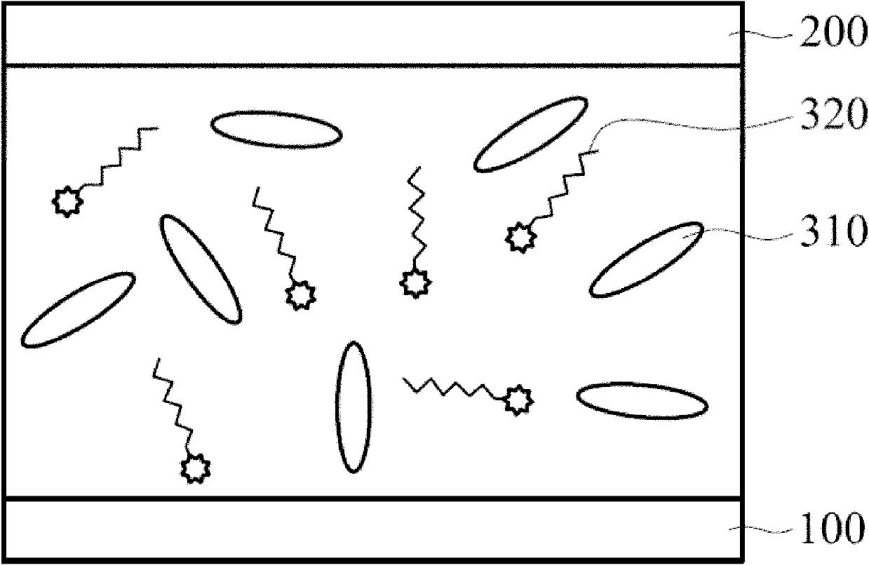
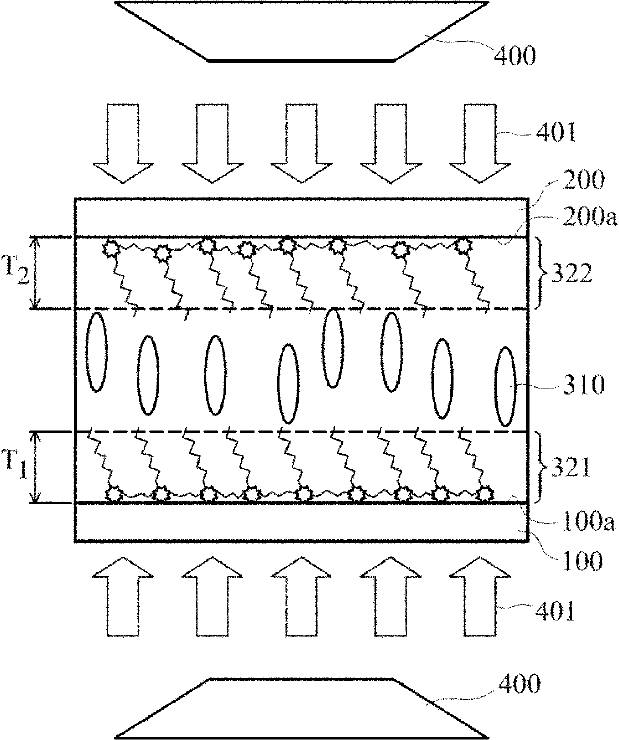
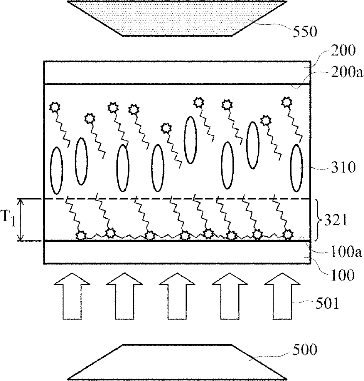
[0029] The present invention provides a method for manufacturing a liquid crystal display, Figure 1 to Figure 2 Process steps of a liquid crystal display according to an embodiment of the present invention are shown. First, see figure 1 , the first substrate 100 and the second substrate 200 are provided, wherein the first substrate 100 and the second substrate 200 are disposed opposite to each other. In one embodiment, the first substrate 100 is a thin film transistor substrate, and the second substrate 200 is a color filter substrate, wherein the thin film transistor substrate 100 further includes pixel control structures such as thin film transistor structures, pixel electrodes, scan lines and data lines ( not shown in the figure).

[0030] After that, the mixed solution is filled between the first substrate 100 and the second substrate 200, and the mixed solution can be injected into the first substrate 100 and the second substrate by one drop filling (ODF) or injection ...


PUM

PropertyMeasurementUnit
thicknessaaaaaaaaaa
wavelengthaaaaaaaaaa
poweraaaaaaaaaa

Abstract

The invention provides a method for producing a liquid crystal display, which comprises the following steps that a first baseplate and a second baseplate are arranged, wherein the first and second baseplates are oppositely arranged; a mixed solution is filled between the first and second baseplates, and comprises a plurality of liquid crystal molecules and a plurality of monomers; and the mixed solution is subjected to an ultraviolet irradiation technology, the monomers are polymerized to form a first alignment control layer on the surface of the first baseplate, which faces the liquid crystal molecules, and a second alignment control layer on the surface of the second baseplate, which faces the liquid crystal molecules, wherein the ratio of the thickness of the first alignment control layer to the thickness of the second alignment control layer is (1:2)-(2:1). According to the method, double-sided ultraviolet irradiation is carried out simultaneously, or the first and second baseplates are alternatively irradiated for reducing the thickness difference of the alignment control layers on the two baseplates, the bright spot problem of the local domain of a liquid crystal display panel can be solved, and further, the process yield is improved.

Description

technical field [0001] The present invention relates to a method for manufacturing a liquid crystal display, and in particular, to a method for manufacturing a liquid crystal display having an alignment control layer. Background technique [0002] Liquid crystal displays (liquid crystal displays) have been applied to various personal computers, personal digital assistants (PDAs), mobile phones, televisions, and the like due to their advantages of light weight, low power consumption, and no radiation. The traditional liquid crystal panel is mainly composed of a pair of substrates and a liquid crystal layer formed between the substrates. Before forming the liquid crystal layer, an alignment layer needs to be coated on the substrate, and then the liquid crystal alignment is completed by a rubbing method. The function of the alignment layer is to make the liquid crystal molecules present a specific arrangement between the substrates, and polyimide (PI) is most commonly used as t...

Claims


Application Information

Patent Timeline
Patent Type & Authority Applications(China)
IPC IPC(8): G02F1/1337G02F1/1333
Inventor 沈宏明杨凯能黄婉玲
Owner INNOLUX CORP
Why Eureka
Try Eureka