

Double-light-beam exposure system and method for manufacturing photonic crystal mask layer
A technology of photonic crystals and exposure systems, applied in microlithography exposure equipment, photolithography exposure devices, optics, etc., can solve the problems of low production efficiency, difficulty in mass production, and high production costs, and achieve high production capacity and easy implementation , low-cost effect
- Summary
- Abstract
- Description
- Claims
- Application Information
AI Technical Summary
Problems solved by technology
Method used
Image

Examples
Embodiment Construction
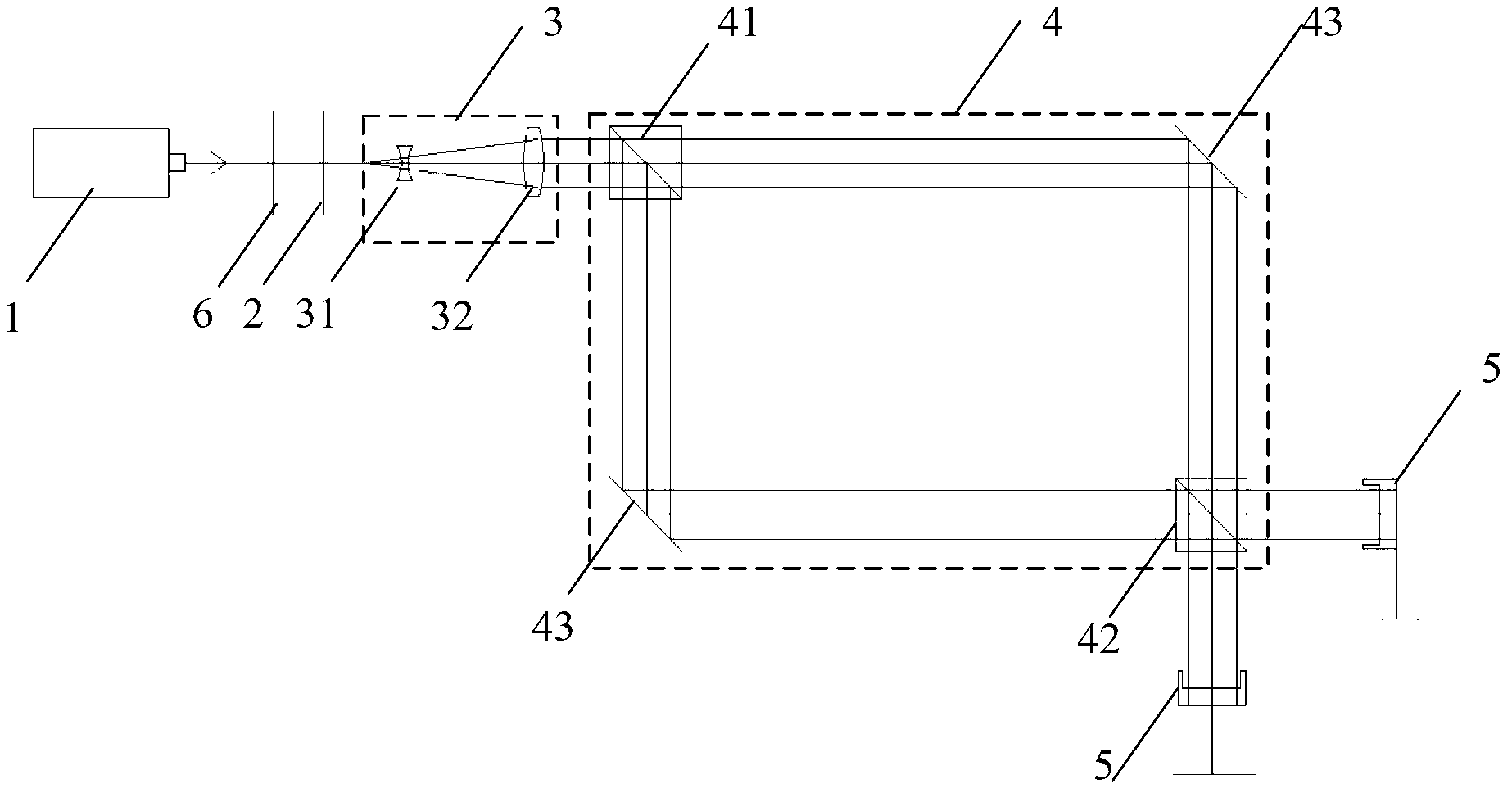
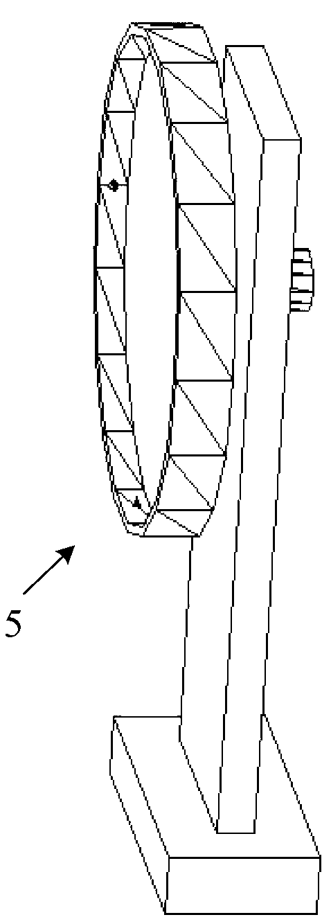
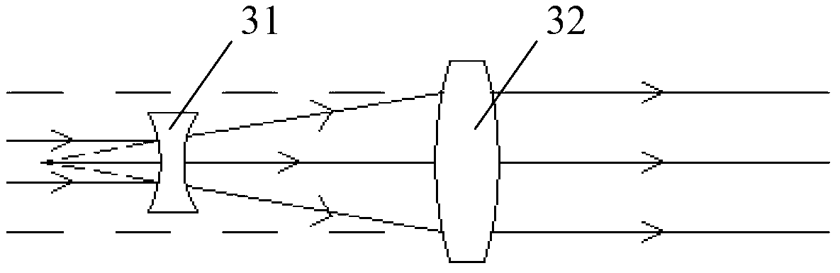
[0043] The following will further describe in detail the double-beam exposure system and method that can be used to fabricate the photonic crystal mask layer of the present invention.
[0044] The invention will now be described in more detail with reference to the accompanying drawings, in which preferred embodiments of the invention are shown, it being understood that those skilled in the art may modify the invention described herein and still achieve the advantageous effects of the invention. Therefore, the following description should be understood as the broad knowledge of those skilled in the art, but not as a limitation of the present invention.
[0045] In order to make the purpose and features of the present invention more comprehensible, the specific implementation manners of the present invention will be further described below in conjunction with the accompanying drawings. It should be noted that the drawings are all in a very simplified form and use imprecise rati...
PUM
 Abstract
Description
Claims
Application Information