Wool preparing process by crystalline silicon based on laser interference induced reaction

A technology of laser interference and crystalline silicon, which is applied in the field of solar photovoltaic applications, can solve the problems of high battery fragmentation rate, difficulty in improving battery efficiency, and inability to prepare polycrystalline silicon wafers with strong alkali solution, so as to achieve the speed of improvement, good industrialization prospects, and avoid disadvantages effect of influence

Inactive Publication Date: 2012-10-03
SUN YAT SEN UNIV
View PDF2 Cites 9 Cited by
  • Summary
  • Abstract
  • Description
  • Claims
  • Application Information

AI Technical Summary

Problems solved by technology

[0006] It can be seen that strong alkali solutions such as sodium hydroxide or potassium hydroxide react with silicon and no toxic gas is released. At the same time, the treatment of this type of waste liquid is relatively easy, and it is not easy to pollute the environment. However, the corrosion of silicon by this type of strong alkali solution is anisotropic Heterotropic, can only form pyramid-shaped suede on the silicon wafer with (100) crystal orientation, but cannot form effective anti-reflection structure at the grains of other crystal orientations, so it is not possible to directly prepare polysilicon with strong alkali solution ...

Method used


Image

  • Wool preparing process by crystalline silicon based on laser interference induced reaction
  • Wool preparing process by crystalline silicon based on laser interference induced reaction
  • Wool preparing process by crystalline silicon based on laser interference induced reaction

Examples


Embodiment 1

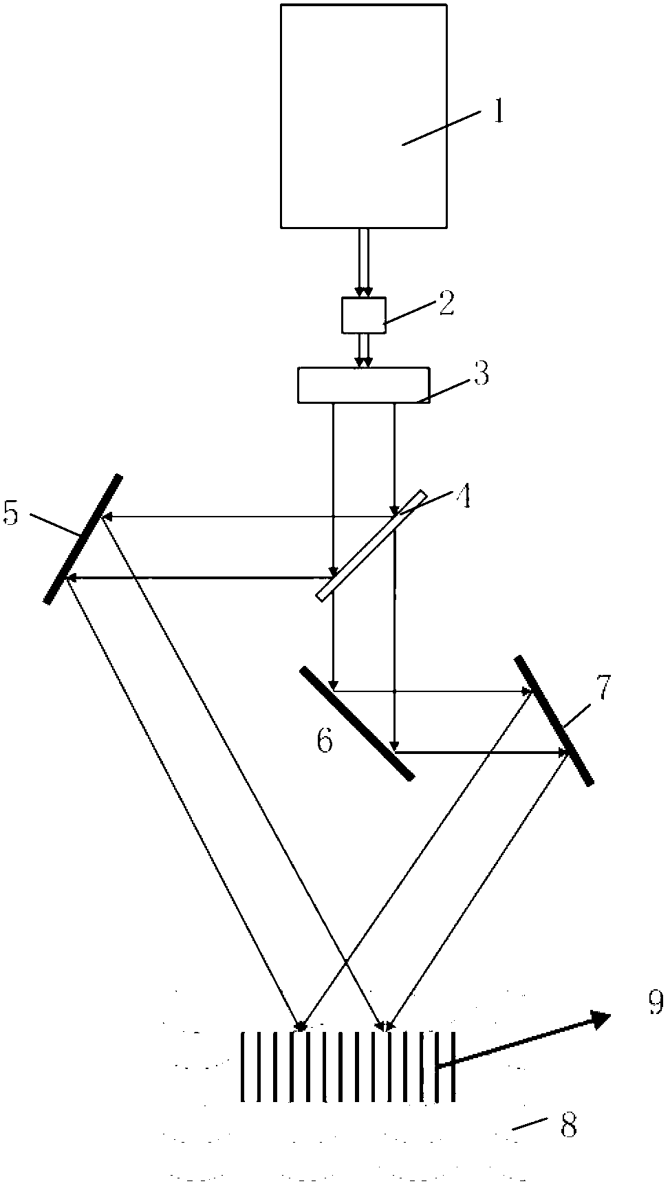
[0031] like figure 1 As shown, a kind of crystalline silicon texturing process based on laser interference induced reaction of the present invention, its specific steps are:

[0032] (1) Etching treatment: removing the mechanical damage on the surface of the sample, i.e. the silicon wafer 9, by etching;

[0033] (2) Put the silicon chip 9 into the strong alkali solution tank 8 equipped with a strong alkaline solution at a certain concentration at room temperature. In this embodiment, the strong alkaline solution can be sodium hydroxide solution, and the strong alkaline solution The temperature is kept at room temperature 25°C or below.

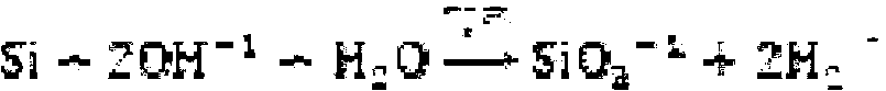
[0034] (3) A chemical reaction occurs by locally heating the crystalline silicon wafer soaked in a strong alkali solution by laser: turn on the laser 1, select the appropriate laser wavelength, pulse frequency, and laser power, and expand the laser beam through the beam expander 2 and 3 After processing, an interference pattern is formed thr...

Embodiment 2

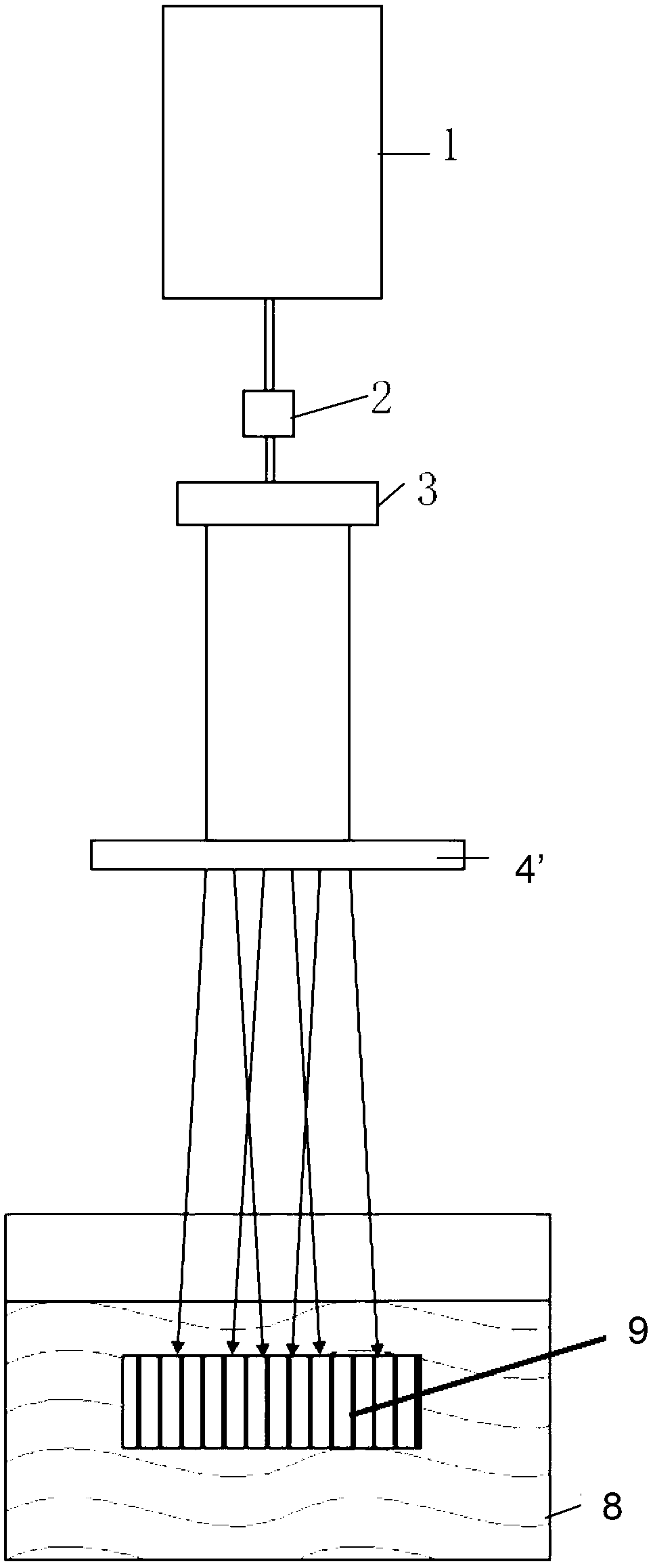
[0037] This embodiment is basically the same as the first embodiment above, the difference is: figure 2 As shown, in the above step (3), the grating 4' is used to replace the beam splitter 4 and the mirrors 5, 6, 7 in the first embodiment to form an interference pattern.


PUM

PropertyMeasurementUnit
Widthaaaaaaaaaa

Abstract

The invention belongs to the technical field of a solar battery, in particular to a wool preparing process by crystalline silicon based on laser interference induced reaction, which comprises the following steps of: (1) corrosion treatment: corroding a silicon wafer to remove mechanical damage on the surface; (2) placing the silicon wafer in an alkaline solution with a certain concentration at room temperature; (3) locally heating the crystalline silicon wafer dipped in strong base solution by laser; and (4) forming a wool face: scanning the whole silicon wafer by interference laser till an uniform wool face is formed on the surface of the silicon wafer. The wool preparing process is free from a laser with over-high power, and saves the energy sources and the machining cost. The process is controlled within an optical spot and has less affect the silicon wafer in other positions. In addition, the preparing process is simple, convenient and rapid. No toxic gases are generated in the wool preparing process, and adverse effects on health of workers and environment are avoided. The wool preparing process by crystalline silicon based on laser interference induced reaction, provided by the invention, can enhance the speed of the process greatly, has good industrialized prospect, and improves the efficiency of the battery extremely.

Description

technical field [0001] The invention belongs to solar photovoltaic applications, in particular to a crystalline silicon texturing process based on laser interference induced reaction. Background technique [0002] The preparation of the textured surface on the surface of the solar cell can effectively reduce the reflection of the solar cell to sunlight, thereby improving the efficiency of the solar cell. [0003] At present, the commonly used texturing process in polycrystalline silicon solar cells is to corrode polycrystalline silicon wafers in a specific ratio of HF / HNO3 solution to form oval or silkworm-shaped corrosion pits on the surface of silicon wafers, thereby reducing the reflection of light, but this method The reflectivity of the prepared crystalline silicon wafer is as high as 20%, which is much higher than that of the pyramid-shaped suede surface prepared by anisotropic etching of single crystal silicon wafer by sodium hydroxide, which is also an important reas...

Claims


Application Information

Patent Timeline
IPC IPC(8): H01L21/268H01L21/306
Inventor 沈辉刘超梁齐兵
Owner SUN YAT SEN UNIV
Why Eureka
Try Eureka