Heterojunction solar cell with buried grid structure
A solar cell and heterojunction technology, applied in circuits, photovoltaic power generation, electrical components, etc., can solve the problem of hydrogenated amorphous silicon attenuation, which has not been well solved, to increase visible light absorption, improve performance, and reduce grids. Effect of Line Shading Area
- Summary
- Abstract
- Description
- Claims
- Application Information
AI Technical Summary
Problems solved by technology
Method used
Image
Examples
Embodiment 1
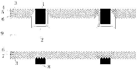
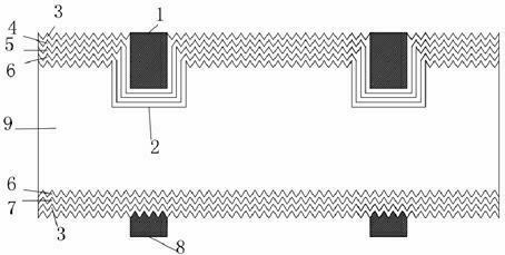
[0015] like figure 1 As shown, a heterojunction solar cell with a buried gate structure includes an N-type single crystal silicon substrate 9, a battery positive electrode 1, a groove 2, an intrinsic hydrogenated nano-silicon film layer 6, a P-type hydrogenated nano-silicon film layer 5, P-type heavily doped hydrogenated nano-silicon carbide film layer 4 , N-type hydrogenated nano-silicon film layer 7 , transparent conductive film 3 , battery negative electrode 8 . The N-type monocrystalline silicon substrate 9 is provided with a groove 2 on the front (main light-receiving surface), and a layer of intrinsic hydrogenated nano-silicon film layer 6, P-type hydrogenated nano-silicon film layer 5 and P-type heavy silicon film layer are sequentially deposited on the front side. Doping hydrogenated nano-silicon carbide film layer 4, and preparing a layer of transparent conductive film 3 on the P-type heavily doped hydrogenated nano-silicon carbide film layer 4; the back of the N-type...
Embodiment 2
[0020] The structure of the heterojunction solar cell with buried gate structure is the same as that in Embodiment 1.
[0021] The preparation method of the buried gate structure heterojunction solar cell in Example 2 is as follows:
[0022] The N-type single crystal silicon substrate 9 used has a thickness of 200 μm and a resistivity of 3Ω·cm. Laser grooves are cut on one side of the N-type single crystal silicon substrate 9 to form grooves 2 with a width of 35 μm and a depth of 18 μm. Then, the grooved N-type single crystal silicon substrate 9 is textured in the mixed solution described in Embodiment 1 to form a pyramid-shaped textured surface. Then, the N-type single crystal silicon substrate 9 after texturing is cleaned and dried by an acid cleaning process, and the surface cleanliness of the silicon wafer is required to be very high. Then use PECVD technology to deposit intrinsic hydrogenated nano-silicon film layer 6 on the front side of N-type single crystal silicon su...
PUM
| Property | Measurement | Unit |
|---|---|---|
| Thickness | aaaaa | aaaaa |
| Doping concentration | aaaaa | aaaaa |
| Thickness | aaaaa | aaaaa |
Abstract
Description
Claims
Application Information

