Bi-polycrystal strain SiGe SOI (Silicon On Insulator) Bi CMOS (Complementary Metal-Oxide-Semiconductor) integrated device and preparation method thereof
An integrated device, dual polycrystalline technology
- Summary
- Abstract
- Description
- Claims
- Application Information
AI Technical Summary
Problems solved by technology
Method used
Image

Examples
Embodiment 1
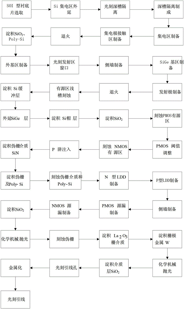
[0118] Embodiment 1: The preparation of a double polycrystalline, strained SiGe SOI BiCMOS integrated device with a channel length of 22nm, the specific steps are as follows:
[0119] Step 1, epitaxial growth.
[0120] (1a) Select the SOI substrate, the support material of the lower layer of the substrate is Si, and the middle layer is SiO 2 , with a thickness of 150nm, and the upper material is doped with a concentration of 1×10 16 cm -3 N-type Si with a thickness of 100nm;
[0121] (1b) Using chemical vapor deposition (CVD), grow a layer of N-type epitaxial Si layer with a thickness of 50nm on the upper Si material at 600°C, as the collector region, and the doping concentration of this layer is 1× 10 16 cm -3 .
[0122] Step 2, deep trench isolation preparation.
[0123] (2a) Deposit a layer of SiO on the surface of the substrate at 600°C by chemical vapor deposition (CVD) 2 ;
[0124] (2b) In the photolithographic isolation area, a deep groove with a depth of 2.5 μ...
Embodiment 2
[0179] Embodiment 2: The preparation of a double polycrystalline, strained SiGe SOI BiCMOS integrated device with a channel length of 130nm, the specific steps are as follows:
[0180] Step 1, epitaxial growth.
[0181] (1a) Select the SOI substrate, the support material of the lower layer of the substrate is Si, and the middle layer is SiO 2 , with a thickness of 300nm, and the upper material is doped with a concentration of 5×10 16 cm -3 N-type Si with a thickness of 120nm;
[0182] (1b) Using chemical vapor deposition (CVD), grow an N-type epitaxial Si layer with a thickness of 80nm on the upper Si material at 700°C as the collector region, and the doping concentration of this layer is 5× 10 16 cm -3 .
[0183] Step 2, deep trench isolation preparation.
[0184] (2a) Deposit a layer of SiO on the surface of the substrate at 700 °C by chemical vapor deposition (CVD) 2 ;
[0185] (2b) In the photolithographic isolation area, a deep groove with a depth of 3 μm is etch...
Embodiment 3
[0240] Embodiment 3: the preparation channel length is the dual polycrystalline, strained SiGe SOI BiCMOS integrated device of 350nm, and specific steps are as follows:
[0241] Step 1, epitaxial growth.
[0242] (1a) Select the SOI substrate, the support material of the lower layer of the substrate is Si, and the middle layer is SiO 2 , with a thickness of 400nm, and the upper material is doped with a concentration of 1×10 17 cm -3 N-type Si with a thickness of 150nm;
[0243] (1b) Using the method of chemical vapor deposition (CVD), grow a layer of N-type epitaxial Si layer with a thickness of 100nm on the upper layer of Si material at 750°C, as the collector region, and the doping concentration of this layer is 1× 10 17 cm -3 .
[0244] Step 2, deep trench isolation preparation.
[0245](2a) Deposit a layer of SiO on the surface of the substrate at 800°C by chemical vapor deposition (CVD) 2 ;
[0246] (2b) In the photolithographic isolation area, a deep groove with...
PUM
| Property | Measurement | Unit |
|---|---|---|
| thickness | aaaaa | aaaaa |
| thickness | aaaaa | aaaaa |
| thickness | aaaaa | aaaaa |
Abstract
Description
Claims
Application Information
 - R&D
- Intellectual Property
- Life Sciences
- Materials
- Tech Scout
- Unparalleled Data Quality
- Higher Quality Content
- 60% Fewer Hallucinations
Browse by: Latest US Patents, China's latest patents, Technical Efficacy Thesaurus, Application Domain, Technology Topic, Popular Technical Reports.
© 2025 PatSnap. All rights reserved.Legal|Privacy policy|Modern Slavery Act Transparency Statement|Sitemap|About US| Contact US: help@patsnap.com