

Method for constructing microelectrode pair array on surface of silicon chip containing hydrophobic silicon column
A silicon wafer surface and hydrophobic technology, applied in the field of constructing micro-electrode pair arrays and nanowires, can solve the problems of unsatisfactory assembly effects, etc., and achieve the effects of easy control, stable properties, and simple equipment
- Summary
- Abstract
- Description
- Claims
- Application Information
AI Technical Summary
Problems solved by technology
Method used
Image

Examples
Embodiment 1
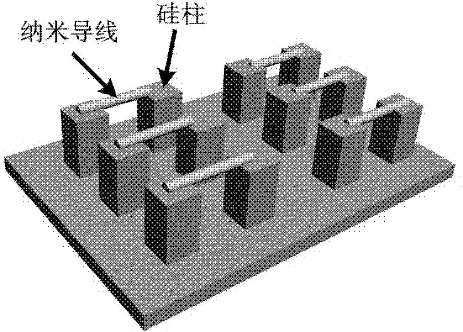
[0033] (1) the silicon chip that adopts laser etching to go out the surface to contain hydrophilic silicon pillar array (the distance between two adjacent silicon pillars in the array and silicon pillar is 15 microns, and the diameter of silicon pillar is micron order standard) soaked in an ethanol solution containing octaalkylfluorosilane with a mass concentration of 1%, and the silicon wafer and octaalkylfluorosilane molecules were grafted for 12 hours, and the octaalkylfluorosilane molecules were modified to On the surface of the silicon chip, obtain a silicon chip containing a hydrophobic silicon column array (the diameter of the silicon column in the array is a micron scale);
[0034] (2) Utilize the effect of gravity to drive the aqueous solution doped with copper nanoparticles with a mass concentration of 1% polyvinyl alcohol and a particle diameter of 10 nm (the mass ratio of polyvinyl alcohol and copper nanoparticles is 1:5) with a speed of 5 cm / s. ) flows through the...
Embodiment 2
[0038] (1) The silicon wafer (the distance between two adjacent silicon pillars in the array and the silicon pillars in the array is 1 micron, the surface of which is prepared by the method of mask plate plus exposure) contains a hydrophilic silicon pillar array, and the silicon pillar The diameter is micron-scale scale) soaked in the acetone solution that contains the dedecyl fluorosilane that mass concentration is 13%, make described silicon chip and dedecyl fluorosilane molecule carry out grafting reaction 1 hour; Decadecyl fluoride Silane molecules are modified to the surface of the silicon chip to obtain a silicon chip containing a hydrophobic silicon column array (the diameter of the silicon column in the array is micron scale);
[0039] (2) Utilizing the adhesion induction technique, use ordinary small cotton swabs to adhere to the concentration of 1×10 -9 The aqueous solution of 3 of % poly 3,4-ethylenedioxythiophene, flows through the top surface of the hydrophobic si...
Embodiment 3
[0041] (1) the silicon chip (two adjacent silicon pillars in the array and the spacing between the silicon pillars in the array is 30 microns, and the diameter of the silicon pillar is Micron scale) soaked into the dimethyl sulfoxide solution containing dodecyl fluorosilane with a mass concentration of 25%, making the silicon chip and dodecyl fluorosilane molecule carry out grafting reaction for 24 hours, the ten Dialkylfluorosilane molecules are completely modified to the surface of the silicon wafer to obtain a silicon wafer containing a hydrophobic array of silicon pillars (the diameter of the silicon pillars in the array is on a micron scale);
[0042] (2) Utilize the action of a magnetic field to drive an aqueous solution containing 20% polystyrene sulfonate-poly 3,4-ethylenedioxythiophene (PSS-PEDOT) at a speed of 1 cm / s to flow at a uniform velocity The top surface of the hydrophobic silicon pillar array on the silicon wafer obtained through step (1), along with the e...
PUM
| Property | Measurement | Unit |
|---|---|---|
| particle diameter | aaaaa | aaaaa |
| particle diameter | aaaaa | aaaaa |
| particle diameter | aaaaa | aaaaa |
Abstract
Description
Claims
Application Information