

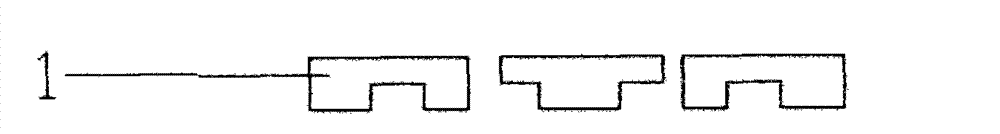
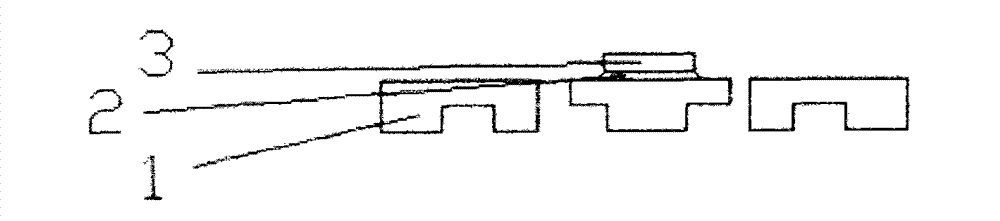
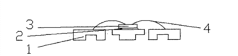
Novel LED (Light Emitting Diode) packaging piece based on DFN (Double Flat No-lead package) and QFN (Quad Flat No-lead Package), and manufacturing method of packaging piece
A technology for an LED package and a manufacturing method, which is applied to electrical components, electric solid-state devices, semiconductor devices, etc., can solve the problems of large product size, damage and deformation of solder joints, and limited application, so as to improve package reliability and reduce product size. Size, the effect of expanding the scope of application
- Summary
- Abstract
- Description
- Claims
- Application Information
AI Technical Summary
Problems solved by technology
Method used
Image

Examples
Embodiment 1
[0027] A method for making a novel LED package based on DFN and QFN is carried out according to the following steps:
[0028] The first step, wafer thinning; wafer thinning thickness is 50μm, roughness Ra 0.10um;
[0029] The second step is to use a double-knife scribing machine and its process for scribing;
[0030] The third step is to use adhesive film to glue the core;
[0031] The fourth step is to use the conventional AAQFN process for pressure welding;
[0032] The fifth step is to use traditional plastic sealing compound 9220 for plastic sealing;
[0033] The sixth step is to use the conventional AAQFN process for post-curing, grinding, tinning, printing, product separation, inspection, packaging, and storage.
Embodiment 2
[0035] A method for making a novel LED package based on DFN and QFN is carried out according to the following steps:
[0036] The first step, wafer thinning; wafer thinning thickness is 130μm, roughness Ra 0.20um;
[0037] The second step is to use a double-knife scribing machine and its process for scribing;
[0038] The third step is to use the film (DAF) on the core;
[0039] The fourth step is to use the conventional AAQFN process for pressure welding;
[0040] The fifth step is to use traditional plastic sealing compound 9220 for plastic sealing;
[0041] The sixth step is to use the conventional AAQFN process for post-curing, grinding, tinning, printing, product separation, inspection, packaging, and storage.
Embodiment 3
[0043] A method for making a novel LED package based on DFN and QFN is carried out according to the following steps:
[0044] The first step, wafer thinning; wafer thinning thickness is 160μm, roughness Ra 0.30um;
[0045] The second step is to use the ordinary QFN scribing process;
[0046] The third step is to use the film (DAF) on the core;
[0047] The fourth step is to use the conventional AAQFN process for pressure welding;
[0048] The fifth step is to use traditional plastic sealing compound 9220 for plastic sealing;
[0049] The sixth step is to use the conventional AAQFN process for post-curing, grinding, tinning, printing, product separation, inspection, packaging, and storage.
PUM
 Abstract
Description
Claims
Application Information