High-temperature large area silicon carbide epitaxial growth device and treatment method

A technology of epitaxial growth and silicon carbide, applied in chemical instruments and methods, single crystal growth, crystal growth, etc., can solve the problems of easy damage and difficult processing, so as to avoid easy damage, expand the range of reaction area and ensure uniformity Effect

Active Publication Date: 2012-10-24
DONGGUAN TIANYU SEMICON TECH
View PDF6 Cites 11 Cited by
  • Summary
  • Abstract
  • Description
  • Claims
  • Application Information

AI Technical Summary

Problems solved by technology

The large-diameter quartz tube is not only easy to damage, but also very difficult to process, which poses a great challenge to the manufacture and safety of the equipment

Method used


Image

  • High-temperature large area silicon carbide epitaxial growth device and treatment method
  • High-temperature large area silicon carbide epitaxial growth device and treatment method
  • High-temperature large area silicon carbide epitaxial growth device and treatment method

Examples


Embodiment Construction

[0039] The present invention will be further described below in conjunction with specific embodiments and accompanying drawings.

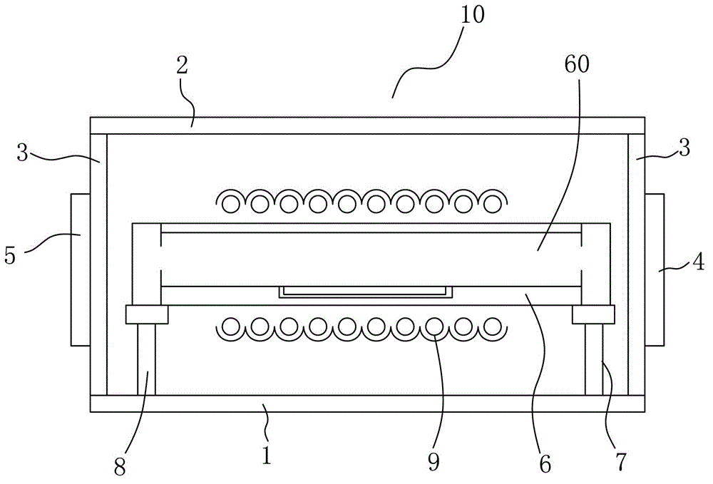
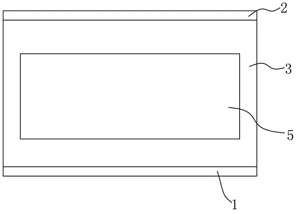
[0040] see Figure 1-2 As shown, this is a specific structure of a preferred example of the present invention, which is a high-temperature large-area silicon carbide epitaxial growth device, including a rectangular parallelepiped (or cube) working chamber 10, the working chamber 10 is composed of: chassis 1, The upper cover 2 and the side wall 3 are surrounded to form a closed space. Wherein, a spare door 4 and a sampling door 5 are respectively arranged on the left and right opposite side walls 3 . Wherein, the sampling door 5 is used to send the sample into the working chamber 10 . The function of the spare door 4 is: when an abnormality occurs in the sampling door 5, related work or maintenance can be continued through the spare door 4 .

[0041] In this embodiment, the chassis 1, the upper cover 2, the side wall 3, the spare door 4 and the s...


PUM


Abstract

The invention discloses a high-temperature large area silicon carbide epitaxial growth device and a treatment method. The high-temperature large area silicon carbide epitaxial growth device comprises a closed working chamber made of stainless steels, a graphite reaction cavity chamber arranged in the working chamber and a heating component arranged at the periphery of the reaction cavity chamber, wherein a tray groove is arranged in the reaction cavity chamber, a tray which bears a silicon carbide substrate is arranged in the tray groove, the reaction cavity chamber is provided with a penetrating channel, and a gas inlet device and a gas outlet device are respectively arranged at two ends of the channel. During treatment, the silicon carbide substrate is put into the reaction cavity chamber and then vacuumized and heated, reaction gas is introduced into the reaction cavity chamber so as to allow epitaxial growth of the silicon carbide, and then the silicon carbide taken out. Compared with the traditional quartz tube structure, the high-temperature large area silicon carbide epitaxial growth device has a simple structure, is relatively easy to manufacture, is convenient to process and can be used for treating the silicon carbide with a larger area. In addition, according to the high-temperature large area silicon carbide epitaxial growth device disclosed by the invention, the working chamber is in a water-cooling stainless steel structure, has higher strength and is not easy to damage.

Description

Technical field: [0001] The invention relates to the technical field of silicon carbide epitaxial growth, and particularly designs a high-temperature large-area silicon carbide epitaxial growth device and a processing method. Background technique: [0002] In recent years, due to the increasing demand for high-temperature resistant and high-power power electronic devices in the fields of military, aerospace, radar communication, power transmission, automotive industry and industrial process control, wide bandgap semiconductors represented by silicon carbide (SiC) increasingly attracting people's attention. SiC is the third-generation semiconductor material after silicon (Si) and gallium arsenide (GaAs) materials. Compared with traditional silicon (Si) materials, SiC has obvious advantages. For example, its forbidden band width is 3 times that of Si, the saturation electron drift rate is 2.5 times that of Si, and the breakdown electric field is 10 times that of Si. Therefor...

Claims


Application Information

Patent Timeline
Patent Type & Authority Applications(China)
IPC IPC(8): C30B25/10C30B25/16C30B29/36
Inventor 孙国胜董林王雷赵万顺刘兴昉闫果果郑柳
Owner DONGGUAN TIANYU SEMICON TECH
Why Eureka
Try Eureka