Single-side three-dimensional circuit chip upside-down-charging packaging-before-etching method and packaging structure thereof

A three-dimensional circuit, sealing first and etching later technology, which is applied in semiconductor/solid-state device manufacturing, circuits, electrical components, etc., can solve the problems of great differences in material characteristics, stress deformation, and reliability levels that affect reliability and safety capabilities. Achieve the effects of not being easy to stress and deform, reducing environmental pollution, and improving safety

Active Publication Date: 2012-10-31
JCET GROUP CO LTD
View PDF4 Cites 2 Cited by
  • Summary
  • Abstract
  • Description
  • Claims
  • Application Information

AI Technical Summary

Problems solved by technology

[0019]3. Glass fiber itself is a kind of foaming material, so it is easy to absorb moisture and moisture due to the storage time and environment, which directly affects the reliability and safety ability or is the level of reliability;
[0020] 4. The surface of the glass fiber is covered with a copper foil metal layer thickness of about 50-100 μm, and the etching distance between the metal layer line and the line can only achieve an etching gap of 50-100 μm due to the characteristics of the etching factor (see Figure 71 , the best production capacity is that the etching gap is approximately equal to the thickness of the etched object), so it is impossible to truly design and manufacture high-density circuits;
[0022]6. Also because the entire substrate material is made of glass fiber, the thickness of the glass fiber layer is obviously increased by 100~150μm, and it cannot be really ultra-thin encapsulation;
[0023]7. Due to the large difference in material characteristics (expansion coefficient) of the traditional glass fiber plus copper foil technology, it is easy to cause stress deformation in the harsh environment process, directly Affects the accuracy of component loading and the adhesion and reliability of components and substrates

Method used


Image

  • Single-side three-dimensional circuit chip upside-down-charging packaging-before-etching method and packaging structure thereof
  • Single-side three-dimensional circuit chip upside-down-charging packaging-before-etching method and packaging structure thereof
  • Single-side three-dimensional circuit chip upside-down-charging packaging-before-etching method and packaging structure thereof

Examples


Embodiment 1

[0114] Embodiment 1, no base island

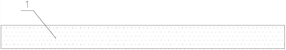
[0115] Step 1. Take the metal substrate

[0116] see figure 1 , take a metal substrate with a suitable thickness, the material of the metal substrate can be changed according to the function and characteristics of the chip, for example: copper, iron, nickel-iron or zinc-iron;

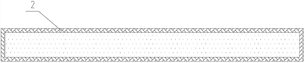
[0117] Step 2. Pre-plating copper on the surface of the metal substrate

[0118] see figure 2 , electroplating a layer of copper film on the surface of the metal substrate, the purpose is to serve as a basis for subsequent electroplating, and the electroplating method can be electroless plating or electrolytic plating;

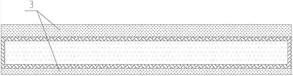
[0119] Step 3: Paste the photoresist film

[0120] see image 3 , using the photoresist film sticking equipment to complete the coating of the photoresist film on the front and back of the metal substrate of the pre-plated copper film in step 2, and the photoresist film can be a wet photoresist film or a dry photoresist film;

[0121] Step 4...

Embodiment 2

[0173] Embodiment 2, there is base island

[0174] Step 1. Take the metal substrate

[0175] see Figure 30 , take a metal substrate with a suitable thickness, the material of the metal substrate can be changed according to the function and characteristics of the chip, for example: copper, iron, nickel-iron or zinc-iron;

[0176] Step 2. Pre-plating copper on the surface of the metal substrate

[0177] see Figure 31 , electroplating a layer of copper film on the surface of the metal substrate, the purpose is to serve as a basis for subsequent electroplating, and the electroplating method can be electroless plating or electrolytic plating;

[0178] Step 3: Paste the photoresist film

[0179] see Figure 32 , using the photoresist film sticking equipment to complete the coating of the photoresist film on the front and back of the metal substrate of the pre-plated copper film in step 2, and the photoresist film can be a wet photoresist film or a dry photoresist film;

[01...


PUM

PropertyMeasurementUnit
thicknessaaaaaaaaaa

Abstract

The invention relates to a single-side three-dimensional circuit chip upside-down-charging packaging-before-etching method, which comprises the following process steps: taking a metal baseplate; pre-plating copper on the surface of the metal baseplate; pasting light resistant films; removing part of the light resistant films on the front surface of the metal baseplate; electroplating an inert metal circuit layer; electroplating a metal circuit layer; pasting light resistant films; removing part of the light resistant films on the front surface of the baseplate; electroplating a metal circuit layer; removing the light resistant films on the surface of the metal baseplate; encapsulating; processing before metallization; electroplating a metal circuit layer; removing the light resistant films on the surface of the metal baseplate; mounting a chip and filling the bottom of the chip; encapsulating; chemically etching; removing the light resistant films on the surface of the metal baseplate; electroplating a metal circuit layer; encapsulating; cutting holes in the surface of plastic packaging materials; washing; mounting balls; and cutting finished products. The method and the structure disclosed by the invention has the benefits that the manufacture cost is lowered, the safety and reliability of the packaged body are improved, and the environment pollution is reduced, so that design and manufacture of high-density circuits are realized actually.

Description

technical field [0001] The invention relates to a single-sided three-dimensional circuit chip flip-chip, first-sealing and then-etching manufacturing method and its packaging structure, belonging to the technical field of semiconductor packaging. Background technique [0002] The manufacturing process flow of the traditional high-density substrate package structure is as follows: [0003] Step 1, see Figure 59 , take a substrate made of glass fiber material, [0004] Step two, see Figure 60 , opening holes at desired locations on the fiberglass substrate, [0005] Step three, see Figure 61 , coated with a layer of copper foil on the back of the glass fiber substrate, [0006] Step 4, see Figure 62 , fill the conductive material in the position where the glass fiber substrate is punched, [0007] Step five, see Figure 63 , coated with a layer of copper foil on the front of the glass fiber substrate, [0008] Step six, see Figure 64 , coated with a photoresist f...

Claims


Application Information

Patent Timeline
Patent Type & Authority Applications(China)
IPC IPC(8): H01L21/56H01L23/31H01L23/00C25D5/10C25D5/02C25D7/00
CPCH01L24/97H01L2224/73204
Inventor 王新潮李维平梁志忠
Owner JCET GROUP CO LTD
Why Eureka
Try Eureka