Touch panel and manufacturing method thereof

A touch panel and manufacturing method technology, applied in the direction of instruments, electrical digital data processing, input/output process of data processing, etc., can solve the problems of poor yield rate, labor-intensive, low production efficiency, etc., to improve output Yield rate, labor cost saving, and fast production speed

Inactive Publication Date: 2012-11-07
许明松
View PDF5 Cites 12 Cited by
  • Summary
  • Abstract
  • Description
  • Claims
  • Application Information

AI Technical Summary

Problems solved by technology

[0009] However, the aforementioned manufacturing methods still have the following deficiencies:
[0010] 1. Poor conductivity: Due to the high price of metallic silver, conductive silver adhesive is usually a mixture of silver powder and adhesive, the ratio of metallic silver is about 30%, sometimes there are defects of poor signal transmission
[0011] 2. The yield rate is not good: the use of screen printing printing method has many control factors, and the quality control is not easy, and the yield rate of the line width of 250 microns is only about 70%, and the narrowest line width is limited to about 200 microns
[0012] 3. Poor alignment: The overprinting method of screen printing is easy to cause misalignment of the wiring contacts of the conductive silver adhesive layer D2
[0013] 4. Low production efficiency: it is a two-stage process, and it needs to be manufactured one by one at the same time, which not only consumes manpower, but also has a slow output rate
[0014] China Taiwan Announcement No. 544824 discloses an invention patent titled "Method for Manufacturing Wires in a Touch Panel". The method forms a first conductive layer on a conductive substrate; forms a first photoresist layer on a first conductive layer; removing part of the first photoresist layer to define a first conductive wiring pattern area on the first conductive layer; using the remaining part of the first photoresist layer as a mask, removing part of the first conductive layer, Until a part of the conductive substrate is exposed; remove the first photoresist layer; the aforementioned method can solve the problems of excessive line width and poor yield, but it is still a two-stage manufacturing method. After completing the aforementioned indium tin oxide conductive layer D1 Afterwards, the exposure, development, and etching processes of the peripheral wiring need to be performed again, and a high-precision mask is required, so there are still shortcomings of slow output rate and high cost.
[0015] China Taiwan Publication No. 201042516 discloses an invention patent titled "touch panel and its manufacturing method". The manufacturing method includes the following steps: forming a transparent conductive layer, forming a metal layer on the transparent conductive layer, Simultaneously patterning the transparent conductive layer and the metal layer, each layer individually produces a first pattern and a second pattern (the second pattern is connected to the outer edge of the first pattern), and removing the first pattern of the metal layer One pattern; the aforementioned method discloses the technical features of simultaneously patterning the ITO layer and the metal layer of the transparent conductive layer, and then removing the metal layer in the visible area, which is more convenient and faster than the previous process, but the use of silver for the metal layer will increase the cost. Using the previous solution The disclosed aluminum metal has the disadvantage that the electrical conductivity is not as good as that of silver metal

Method used


Image

  • Touch panel and manufacturing method thereof
  • Touch panel and manufacturing method thereof
  • Touch panel and manufacturing method thereof

Examples


Embodiment Construction

[0038] In order to further explain the technical solution of the present invention, the present invention will be described in detail below through specific examples.

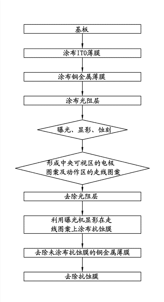
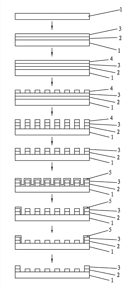
[0039] see figure 1 and figure 2 As shown, the steps of the manufacturing method of the touch panel of the present invention include:

[0040] A. Coating an indium tin oxide thin film 2 on a transparent substrate 1 by means of sputtering or vapor deposition, and coating a copper metal thin film 3 on the indium tin oxide thin film 2 .

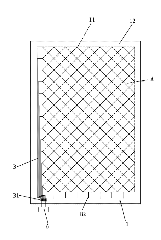
[0041] B. Coating a photoresist layer 4 on the aforementioned copper metal film 3 by using semiconductor etching technology, and after exposing and developing the photoresist layer 4, form each on the aforementioned indium tin oxide film 2 and copper metal film 3 by etching An electrode pattern A is located in a central viewing area 11 of the substrate 1, and a wiring pattern B is located in an action area 12 on the outer edge of the central viewing area 11 and connected to t...


PUM


Abstract

The invention discloses a touch panel and a manufacturing method of the panel. A tin indium oxide thin film and a copper metal thin film are coated on a transparent substrate in sequence, an electrode pattern is formed on each of the tin indium oxide thin film and the copper metal thin film in a central visible area of the substrate with a semiconductor etching technology, a routing pattern is formed in an action area outside the central visible area, an anti-corrosion film is coated in the action area, and the copper metal thin film within the central visible area is dissolved by a special solvent. According to the method disclosed by the invention, the touch panel can be manufactured through a full-etching process.

Description

technical field [0001] The invention relates to a touch panel and a manufacturing method thereof, in particular to a touch panel manufacturing method using a full etching method and the manufactured touch panel. Background technique [0002] The touch panel is a device attached to the liquid crystal display. Its function is to allow the general user to lightly press the touch panel on the display with a finger or a stylus, sense the touch point signal according to different sensing methods, and use the touch The soft board transmits the wire signal of the control panel to the transistor on the main board for interpretation, obtains the coordinate position of the touch point, analyzes the image desired by the user, and displays it on the screen. [0003] Among them, the touch panel sensing methods are roughly divided into resistive touch, capacitive touch, optical touch or ultrasonic touch, etc. Among them, resistive touch and capacitive touch technology are the most mature a...

Claims


Application Information

Patent Timeline
Patent Type & Authority Applications(China)
IPC IPC(8): G06F3/041
Inventor 许明松
Owner 许明松
Why Eureka
Try Eureka