

Method for manufacturing power semiconductor device back
A technology of power semiconductor and manufacturing process, which is applied in the field of backside manufacturing process of power semiconductor devices, and can solve the problems of limited impurity advancement, low diffusion coefficient of conventional impurities, and low activation rate, etc.
- Summary
- Abstract
- Description
- Claims
- Application Information
AI Technical Summary
Problems solved by technology
Method used
Image

Examples
Embodiment Construction
[0015] The present invention will be described in detail below with reference to the accompanying drawings and preferred embodiments of the specification.
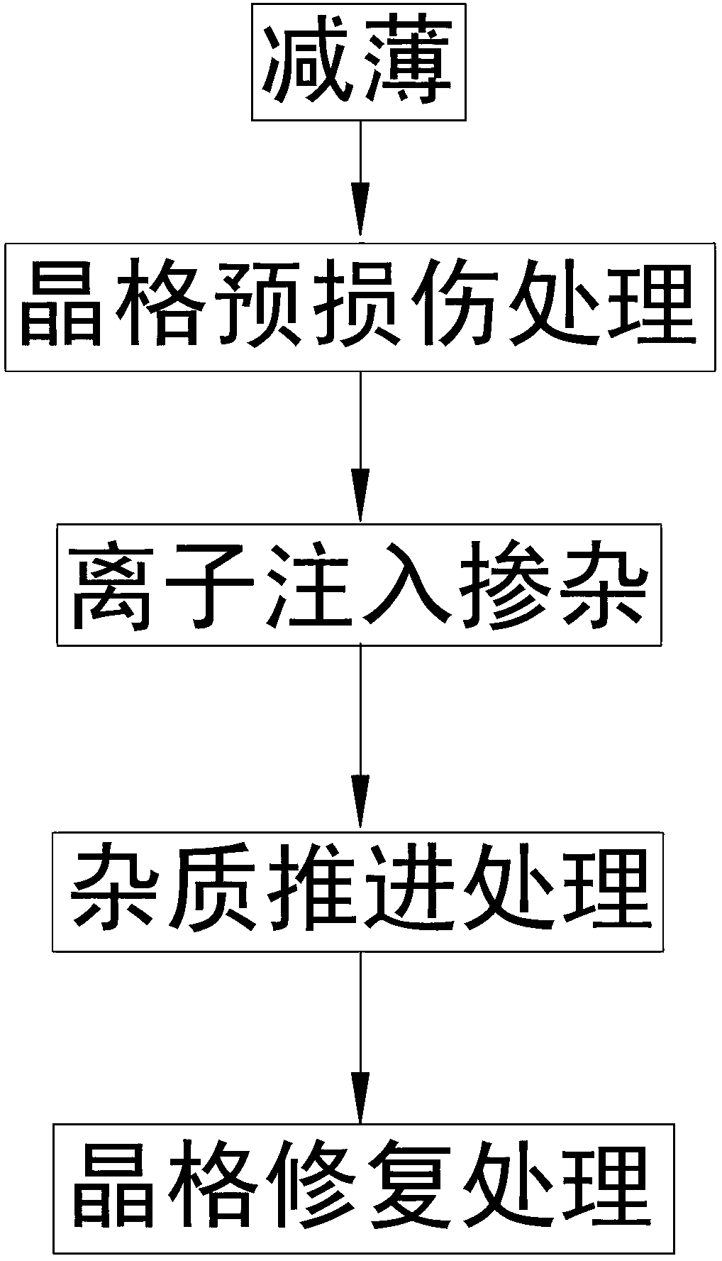
[0016] like figure 1 As shown, the backside manufacturing process of the power semiconductor device of the present invention at least includes the following steps:
[0017] 1.1 The backside thinning process is performed on the silicon wafer with the front-side structure processed.
[0018] 1.2 Perform lattice pre-damage treatment on the back of the silicon wafer to prepare for the subsequent advancement of doping ions. In the wafers with pre-lattice pre-damage, the impurity pushes one to two times deeper than in wafers without pre-lattice pre-damage.
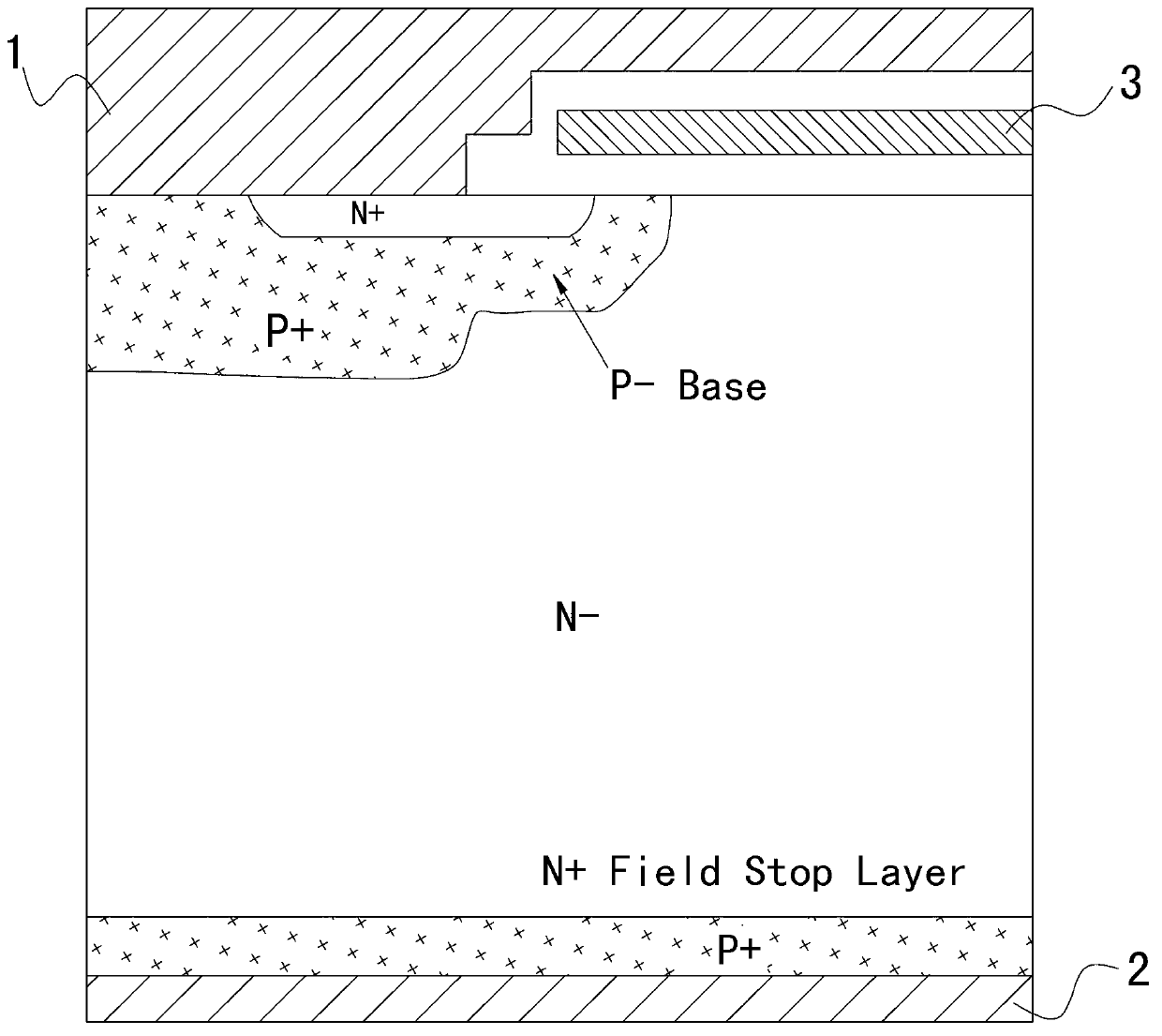
[0019] 1.3 Ion implantation and doping, the N-type or P-type structure is obtained on the back of the chip by the method of impurity doping.
[0020] 1.4 Carry out impurity propelling treatment below 550℃. The low-temperature pushing process can push the impurities impla...
PUM
 Abstract
Description
Claims
Application Information