Eureka AIR delivers breakthrough ideas for toughest innovation challenges, trusted by R&D personnel around the world.

Method for removing impurities through directional solidification with electron beam inducing

An electron beam-induced, directional solidification technology, applied in chemical instruments and methods, inorganic chemistry, non-metallic elements, etc., can solve problems such as inability to remove, reduce process links, facilitate large-scale popularization and application, and reduce energy consumption Effect

Inactive Publication Date: 2012-11-21
DALIAN UNIV OF TECH
View PDF2 Cites 10 Cited by
  • Summary
  • Abstract
  • Description
  • Claims
  • Application Information

AI Technical Summary

Problems solved by technology

[0005] The present invention overcomes the above disadvantages and provides a method for removing impurities by electron beam-induced directional solidification, which is easy to operate and highly controllable, and overcomes the disadvantage that impurities aluminum (Al) and calcium (Ca) cannot be completely removed by one directional solidification. It also improves the energy utilization rate of the electron beam

Method used


Image

  • Method for removing impurities through directional solidification with electron beam inducing

Examples


Embodiment 1

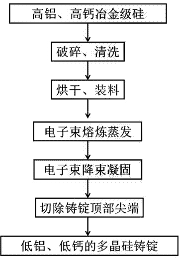
[0021] (1) Retrieving and pretreatment: Select metallurgical grade silicon with an impurity aluminum content of 103ppmw and a calcium content of 42ppmw as raw material, wherein the mass fraction of silicon is 98.5%, break the raw material into small pieces, and place them in analytical pure alcohol for ultrasonication Vibration cleaning to remove residual oil and dust on the surface; the cleaned silicon material is placed in a water-cooled copper crucible in an electron beam melting furnace after drying; the furnace is vacuumed to 1.2 by mechanical pump, Roots pump and diffusion pump ×10-2Pa;

[0022] (2) Evaporation and impurity removal by electron beam smelting: Start the electron gun, set the high voltage to 30kV, and bombard the surface of the polysilicon material with a beam current of 700mA. The state bombards the surface of the silicon material to ensure that the silicon material is heated evenly and stably. Through the observation window, it can be clearly observed tha...

Embodiment 2

[0025] (1) Retrieving and pretreatment: Select metallurgical grade silicon with an impurity aluminum content of 98ppmw and a calcium content of 36ppmw as raw materials, in which the mass fraction of silicon is 99.2%, break the raw materials into small pieces, and place them in analytical pure alcohol for ultrasonication Vibration cleaning to remove residual oil and dust on the surface; the cleaned silicon material is placed in a water-cooled copper crucible in an electron beam melting furnace after drying; the furnace is vacuumed to 1.4 by mechanical pump, Roots pump and diffusion pump ×10-2Pa;

[0026] (2) Evaporation and impurity removal by electron beam smelting: start the electron gun, set the high voltage to 30kV, and bombard the surface of the polysilicon material with a beam current of 600mA. The state bombards the surface of the silicon material to ensure that the silicon material is heated evenly and stably. Through the observation window, it can be clearly observed t...

Embodiment 3

[0029](1) Retrieving and pretreatment: Select metallurgical grade silicon with an impurity aluminum content of 67ppmw and a calcium content of 28ppmw as raw material, in which the mass fraction of silicon is 99.5%, break the raw material into small pieces, and place them in analytical pure alcohol for ultrasonication Vibration cleaning to remove residual oil and dust on the surface; the cleaned silicon material is placed in a water-cooled copper crucible in an electron beam melting furnace after drying; the furnace is vacuumed to 1.1 by mechanical pump, Roots pump and diffusion pump ×10-2Pa;

[0030] (2) Evaporation and impurity removal by electron beam smelting: start the electron gun, set the high voltage to 30kV, and bombard the surface of the polysilicon material with a beam current of 600mA. The state bombards the surface of the silicon material to ensure that the silicon material is heated evenly and stably. Through the observation window, it can be clearly observed that...


PUM


Abstract

The invention belongs to the technical field of polysilicon purification, in particular to a method for removing impurities through directional solidification by adopting the technology of electron beam inducing. The method comprises the following steps of selecting, washing and drying metallurgical grade polysilicon with high aluminum content and high calcium content, placing the polysilicon in a crucible, vacuumizing the polysilicon, starting an electron gun to bombard the polysilicon at a beam flow of 400-700 mA till the polysilicon is totally dissolved to form into a molten pool, and continuously smelting the molten pool for 30-60 min; and then reducing the beam flow of the electron beam by adopting a way of logarithmic beam drop, after the beam flow of the electron beam is reduced to 100-150 mA, stopping droping the beam, the melt slowly freezes to form into an ingot, closing the beam flow to obtain a polysilicon ingot with low aluminum and low calcium contents. According to the method provided by the invention, as the evaporation effect and segregation effect of impurities in the silicon are fully utilized, the complementary advantages of two impurity removing ways of electron beam smelting evaporation and directional solidification can be realized; the aluminum and calcium impurities can be ensured to be removed after one step of smelting so as to meet the performance requirements of a solar cell; the process section is reduced, the energy consumption is reduced, and the method can be in favor of the large-scale promotion and application.

Description

technical field [0001] The invention belongs to the technical field of polysilicon purification, in particular to a method for directional solidification and impurity removal by electron beam induction technology. Background technique [0002] With the development of the global low-carbon economy, the solar photovoltaic industry has ushered in a huge space for development, and the proportion of solar photovoltaic power generation is increasing. According to preliminary statistics, my country added 530,000 kW of grid-connected photovoltaic power generation installed capacity in 2010, and the cumulative installed capacity reached 830,000 kW, of which the cumulative installed capacity of large-scale grid-connected photovoltaic power generation on the ground was 700,000 kW, and the installed capacity of building-integrated grid-connected photovoltaic power generation was about 130,000 kW. . The new installed capacity of the global photovoltaic power generation market in 2010 is ...

Claims


Application Information

Patent Timeline
Patent Type & Authority Applications(China)
IPC IPC(8): C01B33/037
Inventor 谭毅姜大川石爽郭校亮
Owner DALIAN UNIV OF TECH
Why Eureka
Eureka Blog
Learn More