Microfluidic chip for biological chemiluminescence detection and manufacturing method thereof

A microfluidic chip and luminescence detection technology, applied in the field of biochemical detection, can solve the problems of unable to reach the maximum luminous intensity, the scattered light is not fully utilized, and the light detection efficiency is low, so as to improve the light detection efficiency and reduce the loss of scattered light. , the effect of high detection sensitivity

Inactive Publication Date: 2012-11-21
ZHEJIANG UNIV
View PDF9 Cites 19 Cited by
  • Summary
  • Abstract
  • Description
  • Claims
  • Application Information

AI Technical Summary

Problems solved by technology

[0004] At present, the microfluidic chips related to luminescence detection reported in the literature have the following disadvantages: 1. Rely on the microscope platform or the complex optical path composed of lenses and filters: such as the microfluidic chip disclosed in the Chinese patent application number 200910114403.8 A method for measuring substances in a single human red blood cell by chemiluminescence and a biochip fluorescence microspectral detection device and production method disclosed in Chinese patent application number 201110153526.X; The efficiency is low, and the maximum luminous intensity cannot be achieved: such as the microfluidic chip for capillary electrophoresis separation and chemiluminescence detection disclosed in the Chinese patent application number 200910154432.7; 3. The luminescent area is completely transparent, and the scattered light in different directions is not fully utilized. Low light detection efficiency

Method used


Image

  • Microfluidic chip for biological chemiluminescence detection and manufacturing method thereof
  • Microfluidic chip for biological chemiluminescence detection and manufacturing method thereof
  • Microfluidic chip for biological chemiluminescence detection and manufacturing method thereof

Examples


Embodiment 1

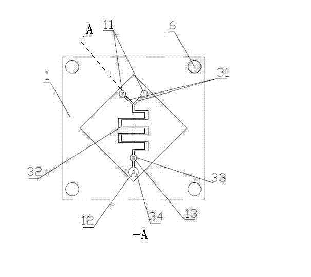
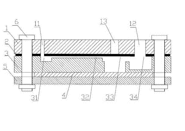
[0031] Such as figure 1 As shown, a microfluidic chip for biochemiluminescence detection, the chip includes an interface layer 1, a light-transmitting layer 2, a channel layer 3, a light-reflecting layer 4 and a fixed layer 5 arranged in sequence from top to bottom, each layer They are bonded together up and down by adhesives and fixed by four sets of fasteners 6. The interface layer 1 is a PMMA material substrate, the thickness of the interface layer 1 is 4mm, and the interface layer 1 is provided with two inlets with a diameter of 1mm. Liquid hole 11, a liquid outlet hole 12 with a diameter of 1.5 mm, an optical fiber connection hole 13 with a diameter of 2.25 mm, the channel layer 3 adopts a PMMA material substrate with a thickness of 3 mm, and the channel layer 3 is provided with two successively connected inlet holes. Liquid flow channel 31, a micro-mixer 32, a detection pool 33, and a waste liquid buffer pool 34, each channel has a width of 2 mm and a depth of 1.5 mm; th...

Embodiment 2

[0038] exist Figure 4 In the shown embodiment, a microfluidic chip for biochemiluminescent detection, the chip includes an interface layer 1, a light-transmitting layer 2, a channel layer 3, a light-reflecting layer 4 and a fixed layer arranged in sequence from top to bottom 5. The layers are bonded together up and down by adhesive and fixed by four sets of fasteners 6. The interface layer 1 is a PMMA substrate, the thickness of the interface layer 1 is 3.5mm, and the interface layer 1 is provided with 3 A liquid inlet hole 11 with a diameter of 1.5mm, a liquid outlet hole 12 with a diameter of 2mm, and an optical fiber connection hole 13 with a diameter of 1.5mm, the channel layer 3 adopts a PMMA material substrate with a thickness of 2.5mm, and the channel layer 3 is provided with Three liquid inlet flow channels 31, a micro-mixer 32, a detection tank 33, and a waste liquid buffer tank 34 are sequentially connected, each channel has a width of 1 mm and a depth of 1 mm; the ...

Embodiment 3

[0045] exist Figure 5In the embodiment, a microfluidic chip for biochemiluminescence detection, the chip includes an interface layer 1, a light-transmitting layer 2, a channel layer 3, a light-reflecting layer 4 and a fixed layer 5 arranged in sequence from top to bottom, each The layers are bonded together up and down by adhesive and fixed by four sets of fasteners 6. The interface layer 1 is a PMMA material substrate. The thickness of the interface layer 1 is 4.5mm. The liquid inlet hole 11, a liquid outlet hole 12 with a diameter of 2.5mm, and an optical fiber connection hole 13 with a diameter of 5mm, the channel layer 3 adopts a PMMA material substrate with a thickness of 3.5mm, and the channel layer 3 is provided with 4 sequentially connected A liquid inlet flow channel 31, a micro-mixer 32, a detection pool 33, and a waste liquid buffer pool 34, each channel has a width of 1.5 mm and a depth of 2 mm; the length of the liquid inlet flow channel 31 is 10 mm, and the fron...


PUM

PropertyMeasurementUnit
pore sizeaaaaaaaaaa
pore sizeaaaaaaaaaa
pore sizeaaaaaaaaaa

Abstract

The invention discloses a microfluidic chip for biological chemiluminescence detection. The chip comprises an interface layer, a transparent layer, a channel layer, a reflecting layer and a fixed layer, which are sequentially arranged from top to bottom. The layers are connected by adhesives and fixed by fasteners; the interface layer is provided with a liquid inlet hole, a liquid outlet hole and an optical fiber interface; the channel layer is provided with a liquid inlet flow channel, a micro mixer, a detecting pool and a waste liquid buffer pool, which are successively communicate with each other; the transparent layer is arranged between the optical fiber interface and the detecting pool; the detecting pool is opened to the lower surface of the channel layer; and the bottom of the detecting pool is connected with the reflecting layer. The invention also discloses a manufacturing method of the microfluidic chip. The microfluidic chip improves reaction luminescence intensity of the detection solution and optical detection efficiency, and has advantages of simple preparation method, convenient operation, fast detection, high sensitivity, and accurate detection result.

Description

technical field [0001] The invention relates to the field of biochemical detection, in particular to a microfluidic chip for biochemiluminescent detection and a manufacturing method thereof. Background technique [0002] At present, in the research of chemistry and life sciences, fluorescence and chemiluminescence are one of the most widely used high-sensitivity quantitative detection methods. Due to the high photon energy absorption efficiency of the fluorophore, the excited fluorophore in the molecule can release a large amount of light energy and generate a high-intensity light signal. Therefore, the pretreatment of the sample is simple and the detection is convenient. However, since the excited sample itself contains complex background fluorescent groups, non-specific excitation fluorescence will be generated, and the complex spectrum of the excitation light source will interfere with the detection of fluorescence light detectors. Therefore, various filter devices are re...

Claims


Application Information

Patent Timeline
Patent Type & Authority Applications(China)
IPC IPC(8): G01N21/76B01L3/00
Inventor 张武明李振煜王酉叶杭庆李光
Owner ZHEJIANG UNIV
Why Eureka
Try Eureka